
Another name for a band Stop Filter is the Notch Filter, which is designed to block and reject all frequencies that fall between its two cut-off frequency points, however all frequencies that are on the outer sides of this range, are allowed to pass through.
A straightforward band-pass filter is created when we combine a simple RC low-pass filter with an RC high-pass filter, which permits the passage of frequencies inside a given range, indicated by two cut-off points. On the other hand, when we combine these low and high pass filters in a different way we get a Band Stop Filter (BSF), which is also called as a band reject filter. Opposite to a band-pass filter, this Band Stop Filter permits some frequencies to pass through but blocks or substantially attenuates frequencies inside a predetermined stop band.
The Band Stop Filter is actually a frequency-selective circuit, which rejects frequencies inside its stop band, as opposed to the band-pass filter, which allows frequencies within the given range. If the stop band is very narrow and there is substantial attenuation over a few Hertz, the filter is known as a notch filter because of the sharp deep notch in the frequency response curve.
Exactly like the band-pass filter, the band stop filter is also a second-order (two-pole) filter which includes two cut-off frequencies. These cut-off frequencies are commonly referred to as the -3dB points or half-power points, which actually defines the bandwidth of the stop band, meaning the range between these two -3dB points.
The function of the band stop filter is to allow frequencies from DC (zero Hz) up to its lower cut-off frequency (fL) to pass through, and also the frequencies above its upper cut-off frequency (fH) to pass through as well, but block all frequencies that lie in between this range. The bandwidth (BW) of the stop band therefore can be defined as: (fH – fL).
For a wide-band stop filter, the actual stop band is situated between the lower and upper -3dB points, which means that it will attenuate or reject all frequencies between these cut-off points, thus creating a frequency response curve with a distinctive notch, in the ideal case, as shown below:
Response Curve Waveform of a Band Stop Filter

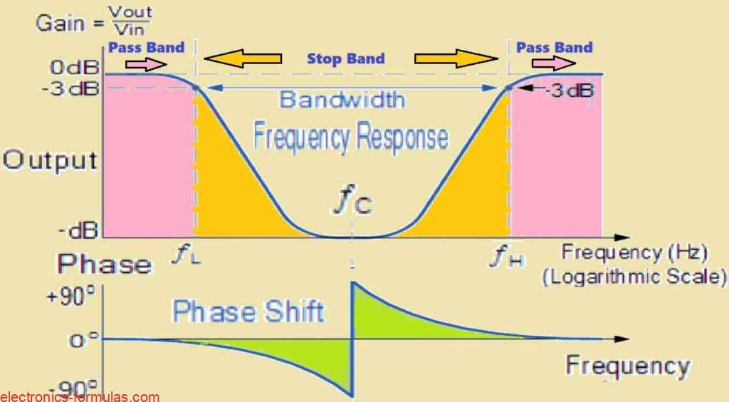
If we examine the amplitude and phase curves of the band stop circuit, we observe that the quantities fL, fH, and fC are just the same as those used in describing the behavior of the band-pass filter.
This observation arises, because the band stop filter functions as an inverted or complementary form of the conventional band-pass filter. This means that the definitions for key parameters such as bandwidth, pass band, stop band, and center frequency remain the same.
Therefore we can apply the same mathematical formulas to determine the bandwidth (BW), center frequency (fC), and quality factor (Q) while calculating the band stop filter just as we do for the band-pass filter circuits.
In an ideal case of a band stop filter, the attenuation level within the stop band would theoretically reach infinity but the attenuation level within the pass bands would be decreased to zero. This would create a vertical, brick-wall-like transition between the two pass bands and the stop band. Because of this, despite the many methods available for designing a band stop filter, they all fundamentally achieve the same objective.
Typically we can design the band-pass filters by arranging a low-pass filter (LPF) in series with a high-pass filter (HPF), but on the other hand, band stop filters are generally constructed by combining the low-pass and high-pass filter sections in a parallel configuration, as illustrated below.
A Standard Band-Stop Filter Circuit


When we combine the outputs of a high-pass and a low-pass filter we get a frequency response that is very different from a band-pass filter. Unlike a band-pass filter which allows a certain range of frequencies to pass through, this combination creates a filter which rejects a specific band of frequencies, which is also known as a notch filter.
The important thing is that the frequency characteristics of these two filter types do not overlap. A low-pass filter attenuates frequencies exceeding its cutoff frequency (fL) whereas a high-pass filter attenuates frequencies below its cutoff frequency (fH).
If we hook up these filters in parallel, frequencies that are below fL will pass through the low-pass filter unchanged, and frequencies above fH pass through the high-pass filter without becoming attenuated. However, both of the filters reject frequencies between fL and fH, producing in a “notch” in the overall frequency response.
To illustrate this, let us imagine a low-pass filter having a cutoff frequency of 200Hz and a high-pass filter having a cutoff frequency of 800Hz.
Now any signal component which falls below the 200Hz mark will pass through the low-pass filter, and any signal that is above 800Hz frequency will pass through the high-pass filter. But the frequencies between 200Hz and 800Hz will be blocked by both filters, and these will be effectively removed from the output signal.
The effects of a band stop filter circuit can be better understood by looking at its characteristics curve, as shown in the following figure.
Characteristics of a Band Stop Filter Circuit


To practically achieve the Band Stop filter characteristic explained above, we may use a simple circuit arrangement. We begin by building separate low- and high-pass filter circuits. To prevent these circuits from interacting, we need to separate them with non-inverting voltage followers, which offer a gain of “1” without loading the prior stage.
We then combine the outputs of these separated filters with a summing amplifier (adder), which is yet another operational amplifier design. This summing amplifier algebraically adds the input signals, allowing the low-pass and high-pass filters’ outputs to be integrated. Then finally we get an output which has the necessary notch filter characteristic due to the combined frequency responses of the separate filters.
Band Stop Filter Circuit Diagram


One useful feature of the operational amplifiers we used in our Band Stop filter design, is their ability to incorporate a voltage gain feature.
We may add amplification to the filter circuit by transforming the non-inverting voltage followers into non-inverting amplifiers, which can be done by including input and feedback resistors into the voltage followers. Then the resultant gain may be calculated using the well-known formula: Av = 1 + Rf/Rin.
Customizing the Notch Filter:
If we need a Band Stop filter with certain cutoff frequencies and attenuation, we can create separate low-pass and high-pass filters to satisfy these specifications.
For example, we can construct a low-pass filter with a cutoff frequency of 1kHz and a high-pass filter with a cutoff frequency of 10kHz to generate a notch filter with -3dB points at 1kHz and 10kHz and a stopband attenuation of -10dB. The intended wideband notch filter can then be created by combining these filters as we learned in our previous discussion.
Because of its flexible design, we can produce highly customized notch filter or Band Stop filter circuits, which can be suitably used for wide range of application and signal processing requirements.
Solving a Band Stop Filter Problem #1
Create a wide band, RC Band Stop filter circuit characterized by lower and upper cutoff frequencies of 190Hz and 790Hz, respectively. Calculate the filter’s geometric mean frequency, bandwidth at the -3dB points, and quality factor (Q).
Solving the problem:
The formula for determining the upper and lower cut-off frequency points of a band stop filter is identical to that of the low and high pass filters, as shown below.
f = 1/2πRC Hz
By taking the value for the capacitor C as 0.1μF for both the filter stages we can calculate the values of the two frequency determining resistors, RL and RH in the following manner:
Low Pass Filter Section
fL = 1/2πRLC = 190 Hz and C = 0.1 μF
∴ RL = 1/(2π * 190 * 0.1 * 10-6) = 8376.57 Ω or 8.5 kΩ
High Pass Filter Section
fH = 1/2πRHC = 790 Hz and C = 0.1 μF
∴ RH = 1/(2π * 790 * 0.1 * 10-6) = 2014.61 Ω or 2 kΩ
Now, it is easy for us to calculate the geometric center frequency fC in the following manner:
fC = √(fL * fH) = √(190 * 790) = 387.42 Hz
fBW = fH – fL = 790 – 190 = 600 Hz
Q = fC/fBW = 387.42/600 = 0.64 or -3.5 dB
With the component values calculated for both the filter stages, we can now integrate them into a single summing amplifier circuit, so that we can finalize the filter design. The output of this adder will then become the algebraic sum of its inputs at any given time.
In order to achieve a straightforward summation without amplification, we can employ resistors with identical values (e.g., 10 kΩ), for both, the feedback resistor and the input resistors in the inverting summing amplifier configuration. With this arrangement we will get a mathematically accurate output which will be the sum of the two input signals.
Finalized Band Stop Filter Circuit Diagram
Thus, now the final circuit diagram for our band stop filter or the band-reject filter as solved above can be drawn as shown below:


So far we have learned that first- or second-order low- and high-pass filters, when connected with a summing op-amp to reject a wide frequency range, may be used to construct simple band-stop filters. On the other hand, we may create band-stop filters with a narrower frequency response to more precisely exclude particular frequencies. We refer to this kind of filter as a notch filter.
Understanding Notch Filters
In the frequency domain, notch filters function essentially like precise instruments.
Their excellent selectivity in attenuating a restricted range of frequencies can be observed by their high Q-factor. These circuits therefore become necessary for carefully eliminating undesired frequency elements.
Imagine a situation where a signal has been polluted by noise, such mains hum, as a result of inductive coupling from devices like ballasts or motors. We may successfully remove the annoying frequency without significantly affecting neighboring frequency components by carefully developing a notch filter that is centered at the problematic frequency. This idea also applies to harmonics, where the signal may be refined by using many notches.
Notch filters are basically a surgical method of frequency-based signal conditioning that may be used to improve signal purity.
These filters are widely used in audio systems where resonant peaks are mitigated in acoustic situations by using variable notch filters. Consider electronic crossovers, synthesizers, and graphic equalizers, all these instruments frequently use notch filters to accurately shape the sound. Because of their versatility, notch filters are among the essential building blocks of signal processing along with its high-pass and low-pass counterparts.
A notch filter’s well defined stopband is what makes it so unique. The Q factor measures this narrow frequency rejection zone which is identical to the resonance behavior in RLC circuits. A higher Q denotes a smaller and deeper notch.
One traditional implementation of the notch filter topology is the twin-T topology. Here, two RC tee networks interconnected in parallel with opposing resistor and capacitor components included in this design. Using this design we can effectively create A deep notch at the specific frequency as desired by us.
Basic Twin-T Notch Filter Circuit


The twin-T notch filter is primarily composed of up of a low-pass circuit and a high-pass filter circuit. The low-pass section is made up of the upper T-pad which is made up of capacitors with two times the capacitance value (2C) and resistors with two times the resistance value (2R).
On the other hand, the high-pass section is formed by the lower T-pad which uses resistors with resistance R and capacitors with capacitance C. The frequency at which these two filter sections interact aggressively, causes the maximum attenuation and this is termed as the notch frequency (fN), which can be calculated using the following formula:
Formula for Calculating Notch Filter Frequency
fN = 1/4πRC
Limitations of the Basic Twin-T Notch Filter
The basic twin-T notch filter has built-in performance limitations. Because of its passive RC architecture, the output is unbalanced which results in a reduced signal levels below the notch frequency than the frequencies that are above the notch frequency.
Furthermore, the filter has a short notch depth due to the Q factor being fixed at a low value of 0.25. These restrictions happen because of phase cancellation caused by the resistive and capacitive components’ identical impedance magnitudes at the notch frequency.
In order to fix these issues and improve filter effectiveness we can use a positive feedback system in the circuit design. Simply by connecting the junction of R and 2C to a voltage divider tapped from the output signal rather than ground we are able to control the amount of feedback. This feedback mechanism directly influences the Q factor of the circuit by allowing a more pronounced and deeper notch depth.
What is a Single Op-amp Twin-T Notch Filter Circuit


The circuit schematic depicts a practical use of the twin-T notch filter with positive feedback. An op-amp buffer separates the filter output from the voltage divider network, which results in an optimal performance for the circuit.
The voltage divider ratio determines the feedback signal, which is injected at the junction of R and 2C in the twin-T network, and this feedback fraction, represented as ‘k’, is critical in determining the filter’s Q factor and hence the notch depth, which can be calculated using the following formula:
k = R4/(R3 + R4)= 1 – (1/4Q)
The ratio of resistors R3 to R4 determines the notch filter’s Q factor. We can simply swap these resistors with a potentiometer coupled with an op-amp buffer that gives you an adjustable negative gain in order to ensure a complete customization of Q.
We can connect the junction of R and 2C straight to the filter output by eliminating the resistors R3 and R4 completely for getting a maximum notch depth at our selected frequency. The above setup maximizes the notch’s depth at the targeted frequency.
Solving another Band Stop Filter Circuit Problem #2
In this problem we want to design a narrow-band, RC notch filter using a couple of op-amps, which must have a center notch frequency, fN of 1.2 kHz and a -3dB bandwidth of 110 Hz. We can use capacitors with values of 0.1 μF in this design in order to calculate the required depth of the notch depth, in decibels.
We have the following figures in hand:
fN = 1200Hz, BW = 110Hz and C = 0.1 μF.
First we will calculate the value of R for the given capacitance of 0.1 μF, as shown below:
R = 1/4πfNC = 1/(4 * π * 1200 * 0.1 * 10-6) = 663 Ω
∴ R = 663 Ω
Next, we will find out the value of Q:
Q = fN/BW = 1200/110 = 10.90 or 11
After this let’s calculate the value of feedback fraction k, as explained below:
k = 1 – (1/4Q) = 1 – 1/(4 *11) = 0.977
Now, we will find out the values of resistors R3 and R4, with the following calculations:
k = R4/(R3 + R4)
0.977 = R4/(R3 + R4)
Let’s assume R4 to be = 12 kΩ, then R3 can be calculated as:
R3 = R4 – 0.977R4
= 12000 – (0.977 * 12000) = 276 Ω
∴ R3 = 276 Ω
Finally, we will calculate the desired notch depth in decibels, dB, using the following calculations:
1/Q = 1/11 = 0.09
fN(dB) = 20log(0.09) = -20.91 dB
Resultant Notch Filter Circuit Diagram using the above Data


Conclusions
From the above tutorial we have noticed that the frequency response of an ideal band stop filter is the opposite of that of a band-pass filter. Between its lower cutoff frequency (fL) and upper cutoff frequency (fH), this filter efficiently filters or attenuates frequencies, allowing only the frequencies that are outside of this range to pass through. The stop band is the range of frequencies that fall between fL and fH in the spectrum.
In order to produce a band stop filter, especially for wideband designs, We can add the outputs of a high-pass and a low-pass filter, with the differential output serving as the filter’s output. A band stop filter containing a wide stop band is commonly referred to as a band reject filter, where as one with a small stop band is known as a notch filter. No matter what we call them, they both come under second-order filter types.
Notch filters specialize in producing significant attenuation at and around a specific frequency range whereas adds a very little attenuation to the remaining frequencies. We use the twin-T parallel RC network as the building block for producing a noticeable notch in notch filter circuit designs. We can also add a feedback network from the output to the intersection of the two T networks in order to boost the Q factor of the filter.
If you want to enhance the notch filter’s selectivity and allow for variable Q values, We can connect the junction of the resistance and capacitance in the two T networks with the center point of a voltage divider network controlled by the filter’s output signal. An accurately built notch filter may provide attenuations more than -60dB at the notch frequency.
Band stop filters are widely used in electrical and communication circuits. As proven, they successfully remove unwanted frequency bands from a system while retaining other frequencies with minimum loss. Because of its great selectivity, notch filters may be used to reject certain frequencies or harmonics that cause electrical noise, such as mains hum, inside a circuit.
References: Band-stop filter
Bandstop filters and the Bainter topology