
So here we are talking about this Common Base Amplifier. Right. That one is just another kind of BJT setup. We also call it Bipolar Junction Transistor. Now in this setup we got this base terminal of the transistor and that one is shared by both the input signal and the output signal. So we say it is common base. That is why this name came.
Now this common base thing is not so famous or used much like the other ones. Like Common Emitter or CE and Common Collector or CC types. But still some people are using it because this one is giving some special kind of input and output characteristics. Which other types are not giving like that.
Ok, so to make this common base type work like an amplifier what we do is we give the input signal to the emitter terminal. Then we take the output from the collector terminal. So in this case the current coming into emitter side is the input current.
And the current going out from the collector side is the output current. But wait. Since transistor is that three layer thing with two pn junctions inside we cannot just apply signals and expect it to work. We must give proper bias to it.
That means if the base emitter junction is forward biased then only it is going to work like a proper common base amplifier.
Now when you see below then you will find that simple diagram showing this common base amplifier basic connection.
Common Base Amplifier Circuit using an NPN BJT

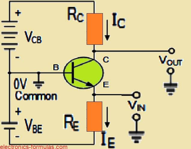
So here we can see from this basic common base configuration that the input side is related to the emitter current which is IE and also that base emitter voltage which is VBE. And the output side is related to the collector current which is IC and that collector base voltage which is VCB.
Now since the emitter current or IE is also working like the input current then any change happening in the input current will make same kind of change in that collector current or IC.
So for this common base amplifier type the current gain which we call Ai is written as iOUT divided by iIN. And that is same like IC divided by IE. So the current gain in this CB configuration is called Alpha or α.
Now in a BJT amplifier the emitter current is always bigger than the collector current because IE is equal to IB plus IC. So the current gain which is α must be smaller than one. Because IC is always less than IE by that IB amount.
So because of this the CB amplifier is not boosting current. It is reducing the current. We also call it attenuating the current. And most common values of alpha go between 0.980 and 0.995.
Now the electrical relationship between all the three transistor currents that is IE IC and IB can be shown like a formula to give us expressions for α which is alpha and β which is beta like shown above.
IE = IB + IC

α = IC / IE
β = IC / IB

Therefore:
IC = α * IE = β * IB

Thus:
α = β / (β + 1)
β = α / (1 - α)

Amplifier Current Gain:
Ai = IOUT / IIN = β / (β + 1) ≅ 1
Thus if a normal bipolar junction transistor had a beta value of 100 then its alpha value would be 100/101 = 0.99.
Voltage Gain of a BJT Amplifier Circuit
So because this common base amplifier type cannot really work like a current amplifier (because Ai is nearly 1), then it must work like a voltage amplifier type. That means it has to boost voltage instead of current.
Now the voltage gain for this common base amplifier is actually the ratio between VOUT and VIN. That means it is collector voltage VC divided by emitter voltage VE.
In simple words, we can say VOUT is same as VC and VIN is same as VE.
Now the output voltage VOUT is created across that collector resistor which we call RC. So the output voltage depends on the collector current IC. From Ohm’s Law we know that VRC = IC multiplied by RC. So if anything changes in the emitter current IE then that will also make collector current IC to change in same way.
Then we can write for a common base amplifier like this:AV = VOUT / VIN
= VC / VE
= (IC * RC) / (IE * RE)Since IC / IE = α, so we can write the voltage gain of amplifier like this:AV = α * (RC / RE)
= Ai * (RC / RE)So because of all this, we can say that the voltage gain is more or less same like the ratio between collector resistance and emitter resistance. But inside a BJT transistor we got one single pn-diode junction that sits between base and emitter terminals. That thing actually brings in something we call the transistor’s dynamic emitter resistance which we write as r’e.

Now for AC signals, this emitter diode junction kind of behaves like it has some small-signal resistance. And that one is given by this formula:
r’e = 25mV/IE.
Here this 25mV comes from thermal voltage of the pn-junction, and IE is that emitter current. So if the emitter current goes up, then r’e goes down by same proportion.
Then we got some of that input current which passes through this internal base-emitter junction resistance and enters base, and also some part goes through that external resistor RE which we connect at emitter side. Now for small-signal calculations, we put both r’e and RE in parallel with each other.
Because r’e is very small and because RE is normally quite big — like in kilo-ohms or so — then the voltage gain of this amplifier keeps changing on its own depending on how much current goes through emitter. So we say that voltage gain becomes dynamic depending on IE.
So if RE is much-much bigger than r’e, then real voltage gain of this common base amplifier will become:
Av = α * Rc / r’e = Ai * [Rc / r’e]
But because we know that current gain is almost equal to one, because Ic is nearly same as IE then we can simply ignore α and write the voltage gain like this:
Av = Rc / r’e
Now for example let us say we got 1mA of current going through that emitter-base junction. Then this junction’s dynamic resistance becomes:
r’e = 30mV / 1mA = 30 ohms
So then if we got collector load resistance as 10k ohms (which is 10000 ohms) then voltage gain Av will be:
Av = 10,000 / 30 = 333.33
So now we can see that, as more and more current flows through that junction, this r’e value goes down. And as r’e goes down, the gain Av goes up automatically. That means higher the emitter current, lower the dynamic resistance and higher the overall voltage gain.
So in same way, if we go on increasing the load resistance then that will also increase the voltage gain of our amplifier directly. But we must also know that in real life, we do not normally use load resistor more than around 20k ohms. That is kind of like the upper limit in practical circuits.
Now depending on what value we choose for Rc, the voltage gain Av for common base amplifier normally stays somewhere between 100 and 2000. It can go up or down but usually it stays inside that range.
Also one more important thing we need to remember is, the power gain of this amplifier is more or less same like the voltage gain only. We can say almost equal.
And since this voltage gain is fully decided by the ratio of two resistances — Rc and r’e — we can clearly say that there is no phase inversion happening here. That means the signal which we feed at the input side (emitter) and the one which we get from the output side (collector), both are in-phase.
So finally we can say this: common base amplifier behaves like a non-inverting amplifier because it keeps the input and output waveforms in same phase.
The Resistance Gain of an Amplifier Circuit
Now one big important thing about this common base amplifier is how its input and output resistances behave and from that only we get one special idea called “resistance gain.” This thing is actually very important because this is what really helps in doing the amplification job.
Like we already saw before, the input is always going into the emitter side and the output is taken out from the collector side, right?
Now if we try to understand how resistance behaves at the input side, we can see two possible resistive paths that go in parallel from the input side to ground. One path is through RE, the emitter resistor that goes directly to ground. And the second path is through that small internal emitter resistance which we call r’e, it goes through base terminal and then to ground.
So if we imagine the base as already grounded and we try to look into the emitter terminal then the total input impedance which we will see becomes:
Zin = RE in parallel with r’e
Or we can just write that as: Zin = RE || r’e
But we have to remember one very important thing — that internal dynamic resistance r’e is much much smaller than the external resistor RE. Like we say, r’e is way less than RE (r’e ≪ RE) so it becomes the main deciding factor in that equation.
Because of this, the overall input impedance becomes very low, almost equal to just r’e only.
That is why, in this common base configuration, the input impedance becomes quite low. Now how low? It will depend on what source impedance Rs we connect to the emitter. Usually the input impedance will come anywhere between around 10 ohms and 200 ohms.
And because of this low input impedance only, this common base amplifier is not used so much as a standalone or single stage amplifier. It becomes limited in that way.
So now let us talk about the output impedance of this common base (CB) amplifier. That output impedance can actually go very high, depending on two main things — one is the collector resistance RC which we use to control the voltage gain and the other is the external load resistance RL which we connect to the output terminal of the amplifier.
Now when we connect that RL at the output side, it goes in parallel with RC. So now these two resistors, RC and RL are both sharing the path and because of that we have to use this parallel formula to find the output impedance:
Zout = RC || RL
But then again, if we make RL much bigger, like way larger than RC — then in that case RC will be the one that controls most of the parallel result. So the output impedance Zout will just become almost same as RC because RL will not do much in that parallel connection. Then we just say:
Zout ≈ RC
So in the common base setup when we check the impedance looking back from the collector terminal, we normally see Zout = RC and that is what we consider as the output impedance.
And because this output impedance can get quite big, this whole common base amplifier acts almost like an ideal current source. That means it takes in current from the emitter side which has very low input impedance and pushes it out through the collector side which has high output impedance.
So due to this kind of behavior, we call this common base amplifier a current buffer or current follower because it kind of passes the same current from input to output but across different impedance levels.
And this is exactly opposite of the common-collector (CC) amplifier which we call a voltage follower because that one keeps the voltage same instead of current.
Conclusions
So in this tutorial where we talked all about the common base BJT amplifier, we came to know many important things. First of all we saw that this amplifier gives a current gain which we also call alpha (α) and that is almost equal to one, or we can say close to unity. That means the output current is almost same as the input current, no big change.
But then when we check the voltage gain, that becomes very high. That gain can go from 100 all the way up to 2000 or even more and this depends on what value of collector load resistor RL we are using in the circuit. Bigger RL, more voltage gain we get.
Then we also saw that this amplifier’s input impedance is very low because it takes input through the emitter side which has that small r’e resistance. But at the same time the output impedance at the collector side can be very high depending on the collector resistor.
Another important thing we learned is that the common base amplifier does not invert the input signal. So if we give a waveform at the input, the output will have the same phase, no upside-down flipping. That means that this is a non-inverting amplifier configuration.
So because of these input-output impedance behaviors — low at input and high at output — this common base amplifier becomes very useful. We use it in audio applications, also in radio frequency (RF) circuits. It can work like a current buffer which means we can connect a low-impedance source to a high-impedance load easily through this amplifier.
Also we can use this amplifier as a single-stage amplifier inside a multi-stage or cascaded amplifier setup, where one amplifier gives its output to the next one. That way we keep the current flow smooth from one stage to another without losing signal strength.
Sources: