So here we are talking about that Phase Splitter circuit which is also one type of BJT means bipolar junction transistor configuration. Now in this type of setup what happens is, we give only one sinusoidal input signal from outside but then this one signal gets divided into two different outputs.
That two outputs come out with a phase difference of 180 electrical degrees from each other means one is like mirror opposite of other in terms of phase.
We apply the input signal into the base terminal of the transistor and then we take one output from the collector side and another output from the emitter side.
So in this way this transistor phase splitter works like a dual output amplifier circuit. It gives us two outputs which are opposite in phase means out-of-phase by 180 degrees, one from collector and one from emitter.
This kind of phase splitter circuit using only one transistor is not something new because we already saw its basic building style in earlier tutorials.
So this phase-inverter or phase splitter kind of combines both features of common emitter amplifier and common collector amplifier. That is because inside this one circuit, we get output from both sides – collector like CE and emitter like CC.
Also like how we bias CE and CC amplifier circuits in forward direction to make it run in linear mode as Class-A amplifier, same way we also bias this phase splitter circuit in forward direction. That way we can reduce the distortion in the output signal and make the amplification more clean.
But before we fully go into this phase splitter topic, let us first refresh our head with how common emitter (CE) amplifier and common collector (CC) amplifier actually work and what are their circuit setups.
Common Emitter Amplifier Circuit
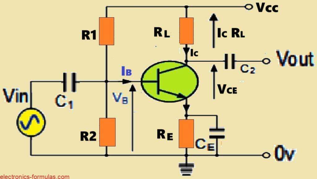
So now we are looking at that common emitter circuit which is using voltage divider for biasing, right. This one is actually the most commonly used type of linear amplifier configuration.
Why? Because it is very easy for us to do the biasing part and also easy to understand how it works so that is why it is very popular.
In this circuit we put the input signal into the base terminal of the transistor and then we take the output signal from across the load resistance which we call RL.
This RL is connected between the collector terminal and the positive supply line which we call VCC. So in this whole setup, the emitter pin becomes common for both input and output sides that is why we call it common emitter.
Now apart from giving us voltage amplification which mainly depends on the ratio of RL divided by RE, the most important thing about this Common Emitter (CE) configuration is that it works like an inverting amplifier.
That means it flips the signal phase, giving a phase reversal of 180 degrees between input and output signals.
To make this CE circuit work properly as a Class-A amplifier, we do proper biasing. That means we adjust it in such a way that the steady current which goes into the base (we call it IB) sets the collector voltage almost at the middle point of the supply voltage.
That middle point we choose because it allows the output signal to move both up and down without distortion.
So the two resistors R1 and R2 which are used in the voltage divider, we select their values very carefully.
We select them in such a way that the transistor gets biased properly. That helps to give us the biggest possible undistorted output signal without any kind of clipping or cutoff problem.
Common Collector Amplifier Circuit
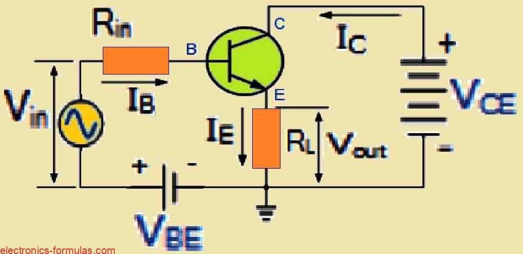
Next we are checking that common collector amplifier circuit. This one is using only one transistor which is wired in common collector mode. That means the collector terminal of the transistor is shared between input side and output side, so it becomes common for both.
In this setup we give the input signal into the base terminal of the transistor, and then we take the output signal from the emitter terminal, just like shown in the diagram.
So here we are not using any collector resistor because the output is not taken from collector, it is taken from emitter. That is why we connect the collector side directly to the supply rail which we call VCC.
This kind of amplifier is also called a voltage follower or more commonly people say emitter follower. Why we call like that? Because the output signal simply follows the input signal, means whatever input comes, almost same thing comes out at output but through emitter.
The main feature of this Common Collector (CC) amplifier is that it does not invert the signal. That means that the input signal passes straight from base-emitter junction and comes out from emitter as it is without flipping. So the output and input signals are “in-phase” they both rise and fall together.
Because of this nature, the voltage gain of this amplifier is slightly less than one. It does not give big voltage amplification like CE amplifier but it gives strong current gain and very low output impedance which is useful in many cases.
Same like how we saw in that common emitter amplifier, here also we do the biasing using voltage divider.
That voltage divider network sets the base voltage roughly at half the supply voltage. So that gives good stability to the DC working point of the transistor and helps the amplifier to run in Class-A mode properly without distortion.
Understanding Phase Splitter Configuration
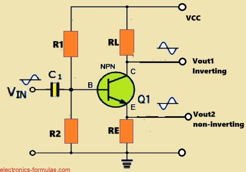
Now if we try to mix up that common emitter amplifier with common collector amplifier and then we try to take the outputs from both sides, one from collector and one from emitter at the same time then we can make a new kind of transistor circuit.
That one gives us two outputs which have same amplitude but the phase is totally opposite, means 180 degrees out from one another.
This type of setup we call Phase Splitter. It is using only one single transistor but still it can give us both inverting and non-inverting outputs as shown in the diagram
We already said before that the voltage gain for common emitter amplifier is given by RL divided by RE, that is -RL/RE. That minus sign tells us the signal is inverted.
Now suppose we select RL and RE to be exactly same in value, like RL = RE then what happens is, the voltage gain becomes -1 which means the output will have same size as input but inverted, so we call it unity gain with inversion.
On the other side, the common collector amplifier which we also call emitter follower, it always gives non-inverting output with gain almost equal to +1 or near unity.
So now if we take one output from collector (inverted) and another from emitter (non-inverted) then we get two signals which have same size but they are 180 degrees opposite in phase. Thats what makes this transistor phase splitter circuit very useful.
We mostly use this kind of phase splitter circuit to give two opposite-phase inputs to another amplifier stage. For example in class-B push-pull power amplifier, we need this kind of anti-phase signals, so this circuit works perfect as a front stage.
Now for all this to work correctly, we must set the DC bias properly. We do that using voltage divider network which is connected across the supply rail and ground.
That voltage divider must be selected in such a way that it gives proper DC voltage at base and allows full symmetrical output swing from both collector and emitter sides. Then only we can get nice clean signals from both terminals with correct phase difference.
Solving a Phase Splitter Problem #1
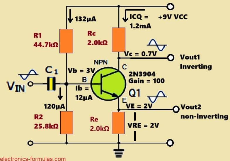
So now we want to design one simple transistor phase splitter circuit that can drive a push-pull power amplifier stage. For that we take one example like this, the supply voltage is 9V, we are using NPN transistor 2N3904, and its Beta value is 100.
Also we take the quiescent collector current to be 1.2mA. Now the input signal is having 1.2V peak amplitude.
Now to stop the distortion on the emitter output side, we must make sure that the emitter voltage, the DC bias, is set higher than that input signal peak. Because if the emitter voltage is too low then the output swing will get chopped and distorted from bottom side.
So here since input peak is 1.2V, we can set the emitter terminal DC voltage to be double of that which means 2.4V. That will make enough headroom and the output from emitter will be clean without any distortion.
So now VE = 2.4V, and the emitter current (which is same like collector quiescent current here), is taken as 1.2mA. Now we calculate the emitter resistance RE by using ohm’s law:
RE = VE / IE = 2.4V / 1.2mA = 2.4 / 0.0012 = 2000 ohms = 2kΩ
So we got RE as 2k resistor. Thats the resistor we put in series with the emitter terminal to drop the DC voltage and set the correct quiescent point.
With this setup we can now build the phase splitter that gives two signals, one from emitter and one from collector, both having equal size but 180 degree opposite phase.
So now if we want the voltage gain of this phase splitter’s common emitter side to be exactly -1, that means unity gain but with phase reversal then we must make the collector load resistor RL same like emitter resistor RE. So RL = RE = 2kΩ.
Now we calculate how much voltage drops across this RL when the quiescent collector current is 1.2mA:
VC = IC × RL = 1.2mA × 2kΩ = 2.4V
So voltage drop across RL becomes 2.4V.
Now to get the actual DC voltage at the collector terminal (VCQ), we subtract this drop from the supply voltage:
VC(Q) = VCC – VC = 9V – 2.4V = 6.6V
So collector sits at 6.6 volts quiescently.
From earlier part, we already set VE(Q) = 2.4V.
So now to find how much VCE the transistor is getting:
VCE(Q) = VC(Q) – VE(Q) = 6.6V – 2.4V = 4.2V
That 4.2V is the collector-to-emitter voltage at idle.
Let us now check this using Kirchhoff’s Law:
VCC – VC – VCE – VE = 0
Substituting:
9 – 2.4 – 4.2 – 2.4 = 0
Yes so it is satisfying KVL and that is expected because both resistors (RE and RL) are same and current is also same (1.2mA) so voltage drop across each resistor is also same, 2.4V.
That confirms the whole DC biasing is perfect, balanced and now both collector and emitter outputs will give us same voltage swing but in opposite direction which is what we need in a phase splitter.
DC Bias Voltages and Base Current Calculation
So now this means that the DC voltage at the emitter output which is the non-inverting side, will be:
VE(Q) = 0V + (IC × RE) = 0 + (1.2mA × 2k) = 2.4V
And the DC voltage at the collector output which is the inverting side, will be:
VC(Q) = VCC – (IC × RL) = 9V – (1.2mA × 2k) = 9 – 2.4 = 6.6V
So both outputs are sitting at different DC voltages which is totally fine in this kind of phase splitter. Both have same current and same resistance so voltage drops are same, but one goes up from ground and other goes down from supply.
Now let us calculate the base current needed for this transistor.
Transistors DC gain (β) is given as:
β = 100
So from formula:
β = IC / IB
Rearranging to find base current:
IB = IC / β = 1.2mA / 100 = 0.012mA = 12µA
So the transistor needs 12 microamps at its base to keep running at 1.2mA collector current.
Finding Voltage Divider Resistors R2 and R1
So now transistor needs 12 microamps into its base and we use the old-school rule that current through the base-to-ground resistor (R2) must be 10 times the base current so that base voltage stays stable and does not fluctuate.
So current through R2 will be:
IR2 = 10 × IB = 10 × 12µA = 120µA
And we already got base voltage:
VB = VE + VBE = 2.4 + 0.7 = 3.1V
Now apply Ohms Law to find R2:
R2 = VB / IR2
= 3.1V / 120µA
= 25833Ω
≈ 25.8kΩ
So we can choose a standard 27kΩ resistor here, no problem.
Now total current flowing through top resistor R1 will be:
IR1 = IR2 + IB
= 120µA + 12µA
= 132µA
And voltage across R1 is:
VR1 = VCC – VB
= 9V – 3.1V
= 5.9V
So again Ohm’s Law:
R1 = VR1 / IR1
= 5.9V / 132µA
= 44696Ω
≈ 44.7kΩ
So nearest standard value is 47kΩ, perfect fit.
Final Answer:
| Parameter | Value |
|---|---|
| Base Voltage VB | 3.1V |
| R2 Current | 120µA |
| R2 Value | 25.8kΩ (use 27kΩ) |
| R1 Current | 132µA |
| R1 Value | 44.7kΩ (use 47kΩ) |
Pluging in the above calculated values in the following diagram gives us our fully completed single transistor phase splitter circuit as shown below:
So here what we doing, this simple single transistor phase splitter thing, it actually gives two same copies of the input signal but with opposite phase.
Like this:
- One output is same phase as the input, means it is not inverted, just like the original signal.
- Other output is completely opposite, means 180 degree flipped so when input is going up, this one goes down.
But both outputs are same in strength or we say equal amplitude, means signal level is almost same.
That’s why, this phase splitter is just perfect for things where we need push-pull or totem-pole style output. Like in audio amplifier or in DC motor driver where one transistor pulls high and other pushes low, like a team.
Now check the circuit shown below, we will explain everything based on that.
Analyzing Totem-pole BJT Output Stage Circuit
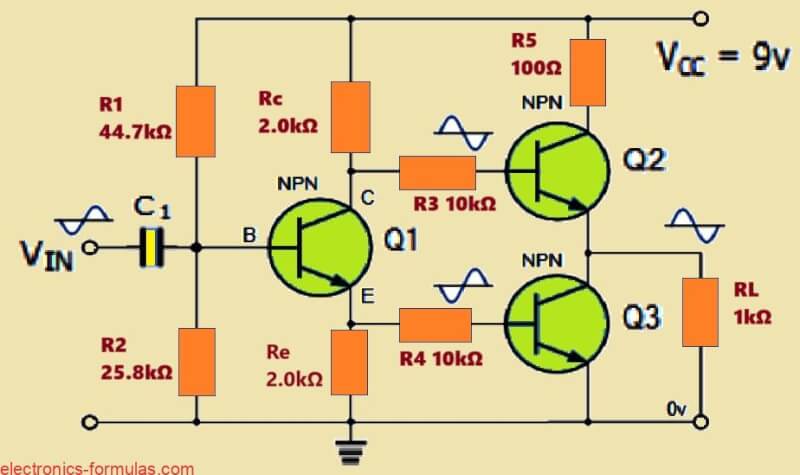
So here in this setup, the output signal is coming out from both collector and emitter sides of the main transistor Q1. We call this thing a totem-pole output ’cause one transistor sits on top of the other just like a pole, and both work one after another.
Now see whats going on step by step:
- When the input signal goes negative, means it is in negative half-cycle, then signal at collector of Q1 becomes positive due to 180 degree flip.
- That time, the upper transistor Q2 gets forward biased, means it turns ON.
- But at same time, lower transistor Q3 stays OFF. So only Q2 is active.
- Now since Q2 is ON, it passes this negative half part of the signal to the load resistor RL. That is how negative side of signal reaches the output.
Then,
- When the input signal goes positive, it is in positive half-cycle so the emitter of Q1 sees that directly (not inverted).
- This time, lower transistor Q3 gets forward biased, so it turns ON.
- But Q2 stays OFF now because it sees negative at its base side.
- So now only Q3 is active and it pushes the positive half of the signal to the same load resistor RL.
So what we get? Like a push-pull action:
- First Q2 pushes negative half,
- Then Q3 pulls positive half,
- They both never ON together, always one ON at a time, controlled by Q1’s collector and emitter sides.
That is why this totem-pole style is super good for strong output swing with proper phase and no clash between Q2 and Q3.
Finally both halves, negative from Q2 and positive from Q3, get added and appear as a clean full waveform across RL, but it is inverted version of the input signal.
Also one more thing, this RL load resistor is not floating randomly, it sits with a DC bias voltage which is kind of centered between the voltages at collector and emitter of Q1.
And that R5 resistor at top, that guy’s job is to control the max current so no short or overheating happens. It saves the transistors from frying.
Conclusions
We are using one NPN transistor Q1 to split one input signal into two opposite signals – one from collector (inverted), one from emitter (non-inverted). This makes it a phase splitter.
How phase splitter works?
Input goes into base of Q1 through C1.
Collector gives 180-degree inverted signal.
Emitter gives same-phase signal.
Amplitudes are similar if RC = RE.
So from Q1 we get two outputs with opposite phase. Perfect for push-pull or totem-pole stages.
How totem-pole stage works?
Collector output of Q1 drives Q2.
Emitter output of Q1 drives Q3.
When Q2 is ON, Q3 is OFF → negative half passes to RL.
When Q3 is ON, Q2 is OFF → positive half passes to RL.
So only one transistor conducts at a time, clean push-pull action.
Final output across RL is inverted full waveform.
R5 controls max current.
With just Q1, Q2, Q3 we build a solid phase splitter + push-pull driver. Very simple but powerful. Works for audio amps, motor drivers, inverters, etc.
Leave a Reply