The common emitter class-A amplifier is specifically engineered to generate a significant output voltage swing even when it is fed with a relatively minuscule input signal voltage that might only be a few millivolts.
These amplifiers are primarily utilized as what we call “small signal amplifiers” a concept we explored in our earlier tutorials.
Now there are instances when you might need an amplifier that can handle larger resistive loads like driving a loudspeaker or powering a motor in a robotic application.
For these kinds of scenarios where you require high switching currents you will need to turn to Power Amplifiers.
The primary role of a power amplifier often referred to as a “large signal amplifier” is to deliver power to the load.
This power is essentially the result of multiplying voltage by current.
In simpler terms while a power amplifier does function as a voltage amplifier the key distinction lies in the fact that the load resistance connected at the output tends to be relatively low.
For example when dealing with loudspeakers that typically have impedances of 4Ω or 8Ω this results in substantial currents flowing through the collector of the transistor.
Due to these elevated load currents it is crucial for the output transistor(s) used in power amplifier stages like the well-known TIP3055 to possess higher voltage and power ratings compared to those transistors that are generally employed in small signal amplifiers such as the BC547.
Now we are really focused on getting the most AC power to our load while trying to use as little DC power as we can from the supply.
This means that we are primarily interested in how efficient the amplifier is at converting power which is often referred to as “conversion efficiency.”
Now here’s the kicker, one of the biggest downsides of power amplifiers, particularly Class A amplifiers is that they tend to have a pretty low overall conversion efficiency.
Why?
Because they draw large currents which leads to a significant amount of power being wasted as heat.
When we talk about efficiency in amplifiers we define it as the root mean square (r.m.s.) output power that’s actually delivered to the load divided by the total DC power drawn from the supply.
Formula for Calculating Power Amplifier Efficiency
This relationship is shown in the following formula:
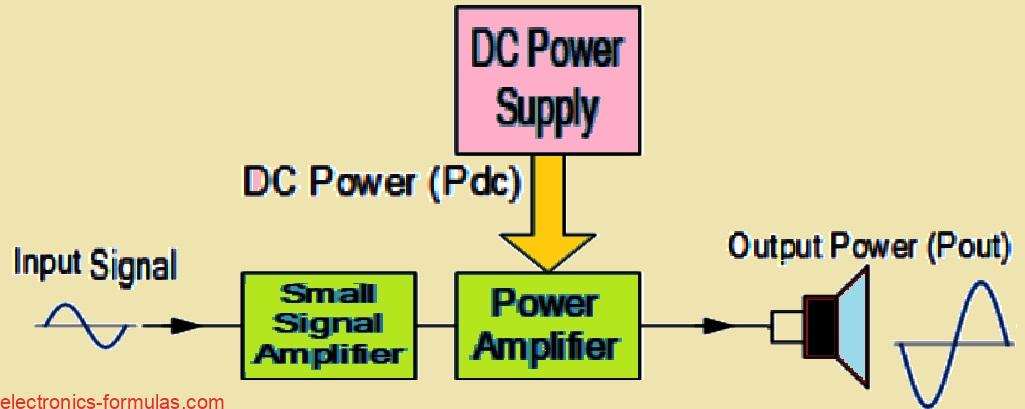
η% = (POUT/PDC) *100%
- In the above formula,
- η% indicates the efficiency of the amplifier.
- Pout refers to the amplifiers output power delivered to the load.
- Pdc represents the DC power taken from the supply.
For a power amplifier to function optimally it is absolutely crucial that the design of its power supply is top-notch ensuring that it can deliver the highest possible continuous power to the output signal without any hiccups.
Class A Amplifier
When we talk about power amplifiers, the Class A Amplifier stands out as the most frequently utilized configuration.
Essentially a Class A amplifier is the most straightforward kind of power amplifier.
It operates using a single switching transistor set up in a typical common emitter circuit configuration which we have discussed before.
This setup is designed to produce an inverted output.
The main feature here is that the transistor is always biased “ON” meaning it remains active throughout the entire cycle of the input signal waveform.
This constant conduction results in a minimal distortion and maximizes the amplitude of the output signal.
What this boils down to is that the Class A Amplifier configuration represents an ideal operating mode.
Since the transistor is always on, there is no risk of crossover or switch-off distortion affecting the output waveform even during the negative half of the cycle.
In terms of design Class A power amplifier output stages may utilize either a single power transistor, or pairs of transistors, working together to handle the high load current effectively.
To illustrate this concept further consider the Class A amplifier circuit depicted below:
Analyzing a Single Stage Class-A Amplifier Circuit
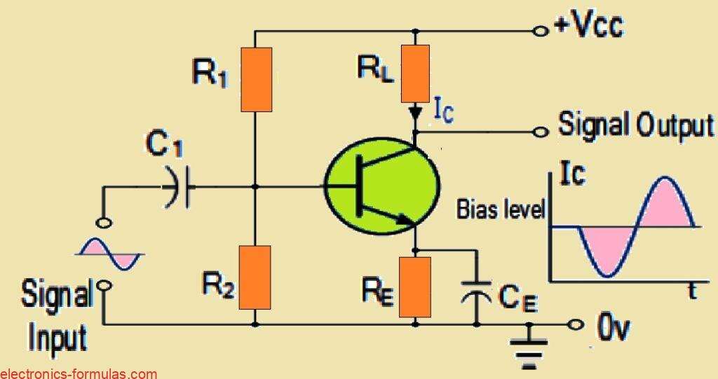
Let’s check out the one of the most straightforward types of Class A power amplifier circuits as shown above.
This particular design features a single-ended transistor that serves as its output stage and it has a resistive load thats hooked up directly to the Collector terminal.
So when the transistor is turned “ON” it effectively sinks the output current through the Collector.
This action leads to an unavoidable voltage drop across the Emitter resistance which in turn limits how much negative output capability we can achieve.
Now when we talk about efficiency, this kind of circuit isn’t exactly winning any awards, it’s quite low typically coming in at less than 30%.
This means that it delivers only a small amount of power while drawing a significant amount from the DC power supply.
One thing to keep in mind is that a Class A amplifier stage continues to pass the same load current even when there’s no input signal present.
Because of this constant current flow, large heatsinks become essential for keeping those output transistors cool.
But wait, if you’re looking for a simple yet effective way to boost the current handling capacity of this circuit while also achieving greater power gain, then you might want to consider swapping out that single output transistor for a Darlington Transistor.
These nifty devices essentially combine two transistors into one package: you have got a smaller “pilot” transistor paired with a larger “switching” transistor.
The fantastic thing about using Darlington Transistors is that they provide a suitably high input impedance while keeping the output impedance relatively low.
This combination helps to minimize power loss and subsequently reduces heat generated within the switching device.
Exploring the Current Gain in Darlington BJTs
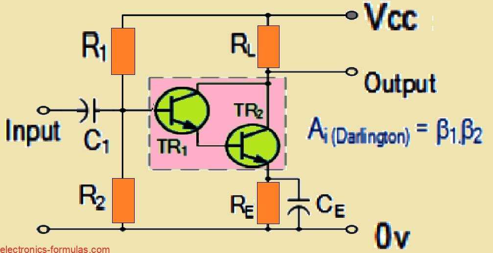
When we talk about the overall current gain, often represented as Beta (β) or hfe value of a Darlington device, it’s pretty fascinating.
Essentially this value is calculated by taking the product of the gains from the two individual transistors and multiplying them together.
This means that, compared to a standard single transistor circuit, the Darlington devices can achieve some impressively high β values along with substantial Collector currents.
Now if we are looking to enhance the full power efficiency of a Class A amplifier then there’s a neat trick we can employ.
By designing the circuit with a transformer that’s directly connected in the Collector circuit, we create what is known as a Transformer Coupled Amplifier.
This clever setup allows the transformer to boost the efficiency of the amplifier by effectively matching the impedance of the load to that of the amplifier’s output.
This matching is accomplished using the turns ratio (n) of the transformer.
To illustrate this concept further let me provide you with an example below.
Class-A Amplifier Circuit with Transformer-coupled Output
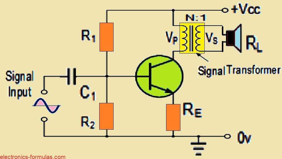
So when the Collector current, often denoted as Ic, drops below the quiescent Q-point established by the base bias voltage—this can happen due to fluctuations in the base current—something interesting occurs.
The magnetic flux within the transformer core starts to collapse and this collapse generates an induced electromotive force (emf) in the primary windings of the transformer.
As a result we see an instantaneous spike in the collector voltage which can actually soar to a value that’s twice the supply voltage or 2Vcc.
This means that when the Collector voltage hits its minimum point, we can achieve a maximum collector current that is also twice Ic.
Now with all this in mind we can go ahead and calculate the efficiency of this particular Class A amplifier configuration using some straightforward equations:
The r.m.s. Collector voltage can be calculated using the following formula:
VCE = (VC(max) – VC(min)) / (2√2) = (2VCC – 0) / (2√2)
The r.m.s. Collector current can be calculated using the following formula:
ICE = (IC(max) – IC(min)) / (2√2) = (2IC – 0) / (2√2)
The r.m.s. Power delivered to the load (Pac) can be therefore calculated as:
Pac = VCE × ICE = (2VCC / 2√2) × (2IC / 2√2) = (2VCC × 2IC) / 8
The average power pulled from the supply (Pdc) can be determined as:
Pdc = VCC × IC
The efficiency of a Transformer-coupled Class A amplifier can be calculated using the following formula:
η(max) = Pac / Pdc = (2VCC × 2IC) / (8VCC × IC) × 100%
The Role of Output Transformers in Amplifier Efficiency
Now let’s talk about how an output transformer can really boost the efficiency of an amplifier.
Basically it does this by matching the impedance of the load to that of the amplifier’s output impedance.
When you use an output or signal transformer that has a suitable turns ratio you can actually achieve Class A amplifier efficiencies that reach up to 40%.
In fact most commercially available Class A type power amplifiers are designed with this kind of configuration in mind.
But since transformers are inductive devices, it’s generally a good idea to steer clear of using inductive components in amplifier switching circuits.
Why?
Because any back electromotive forces (emf) that get generated could potentially harm the transistor if there is not adequate protection in place.
Another significant drawback of this transformer-coupled Class A amplifier circuit is the added cost and bulkiness of the audio transformer that you need.
These transformers can take up quite a bit of space and add to the overall expense of your setup.
Now let’s understand what determines the “Class” or classification of an amplifier.
This classification really hinges on the conduction angle which refers to the portion of the full 360 degrees of the input waveform cycle during which the transistor is actually conducting.
In a Class A amplifier this conduction angle is a complete 360 degrees meaning it conducts for 100% of the input signal.
In contrast other amplifier classes have transistors that conduct for a smaller portion of that angle.
If you are looking for greater power output and efficiency beyond what a Class A amplifier can provide, one effective approach is to use two complementary transistors in the output stage.
This setup involves one transistor being an NPN or N-channel type and the other being a PNP or P-channel type (essentially its complement).
When these two are connected in what’s known as a “push-pull” configuration then you can achieve impressive results!
References:
Leave a Reply