
A digital buffer works in the same way like the NOT gate but with a distinct function. Although we find that a NOT gate (or inverter) generates an output which is just the inverse of its input, meaning that if we supply the input with a “HIGH” logic, then its output turns logic “LOW,” and vice versa, but the digital buffer does not work to alter the signal. Instead it maintains and makes sure that input logic state is same as at its output.
Basically, the primary work of a digital buffer is to isolate logic gates from one another so that the user is able to drive higher loads for example such as relays, solenoids, and lamps, without affecting the input signal. In simple terms we can say that a digital buffer allows the input signal from its input terminal to its output terminal to pass through unchanged, which makes it invaluable when you need to manage different types of circuits without introducing inversion.
So the single-input, single-output NOT gate (such as the TTL 7404) works differently, because it inverts or complements its input signal at the output, whereas a digital buffer does not perform any type of inversion or logical operations. Instead it simply reproduces the input signal at its output, wherein the input signal can have negligibly low current while the output has sufficient current to drive any external load such as a relay, BJT, LED etc. In other words we can say that a digital buffer generates an output which is exactly the same as the signal it supplied at its input, but with a high input impedance and a low output impedance.
We can consider the digital buffer gates as idempotent gates in accordance to Boole’s Idempotent Law, because they do not alter the input signal. They are “non-inverting” devices, and their Boolean expression can be represented as: Q=A.
So now we can define the logical operation of a single input digital buffer as depicted in the following statement.
“Q is true, only when A is true”
It simply means that the output ( Q ) state of a buffer logical gate will be only true (logic “1”) when its input logic level A is true, if not then its output will be false (logic “0”).
Symbol and Truth Table of a Single Input Digital Buffer
Symbol

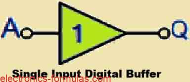
Truth Table
| A | Q |
| 0 | 0 |
| 1 | 1 |
Its Boolean Expression can be written as Q = A and we can read this as: A gives Q
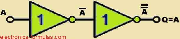
How to use NOT Gates to Replicate Digital Buffer through Double Inversion
It is also possible to create the Digital Buffer by connecting two NOT gates with each other as shown in the following figure. Here, the first NOT gate will “invert” the input signal A and then the second NOT gate will again “re-invert” it back to its original logic level causing a double inversion operation of the input logic signal.

Now, you might be wondering how can a Digital Buffer be useful especially because it does not invert or alter its input signal like a NOT gate, nor does it perform any logical operations as AND or OR gates do. So in this situation it might seem that why not use a simple piece of wire instead which could serve the same purpose as a digital buffer. Well, I understand that is a valid point. However, if you delve deeper you will see that a non-inverting Digital Buffer gate may provide a number of benefits in digital electronics beyond just signal transfer.
One of the key advantages of a Digital Buffer is that we can use it for digital amplification. We can also use it to efficiently isolate several logic gates or circuit stages, and thus ensuring that one circuit’s impedance does not get impacted by another circuit’s impedance.
This type of isolation is essential in complicated circuits which helps to provide a guaranteed steady and dependable functioning.
Furthermore, you may find that Digital Buffers are especially effective when it comes to driving high-current loads, from example like transistor switches, simply because their output current drive capacity surpasses their input signal need.
To explain this in another way we can say that Digital Buffers can be used to magnify a digital signal so that its becomes capable of handling bigger loads due to their strong “fan-out” capabilities, which makes them very useful for certain specific electronic applications.
Understanding Digital Buffer Fan-out Operation

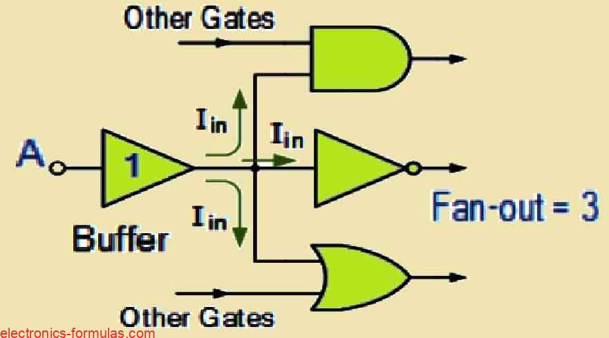
We can define the Fan-out parameter as the output current handling or delivering capacity of a logic buffer gate or any other logic gate enabling the input signal the capability to be amplified at the output of the gate. If you want a specific logic gate to be capable of delivering an increased amount of current to the load then you would need to connect multiple buffer logic gates in parallel to the output of the other logic gate which is configured with an input signal. For example suppose you want to drive a high current load like an LED, then you could think of connecting a few Buffer gates in parallel.
You may find that sometimes the output of a logic gate is integrated to the inputs of other gates, in which every input of the gates call for a certain amount of current from the gate output to ensure that it change logic state correctly. Because of this increase in the number of gates causes the load on the gate to increase also. Therefore the fan-out refers to the number of loads that may be connected in parallel and could be driven together using a single digital buffer gate of logic gate. This type of buffer gate that is designed to work as a current source may have a high fan-out rating that may include up to 20 gates from the same logic family.
When we work with digital buffers, a high fan-out rating tells us that the buffer can drive many outputs at once by providing a substantial amount of current. For us to achieve this the buffer also needs to have a high fan-in rating which means that it should be able to handle a large number of inputs.
But we must be aware that as we increase the fan-inᅳby connecting more inputs to the gateᅳthe propagation delay of the gate increases significantly. Propagation delay is actually the time it takes for a signal to travel from the input to the output, so when we are working with gates that have a fan-in greater than 4, the delay could become quite bigger and that is why we normally avoid using gates with such high fan-in to prevent problems with its performance.
Furthermore, we can also face practical limits on how many inputs and outputs we can connect together. In order to address this issue and stop the problems like signal interference or very high loading, we use devices such as Tri-state Buffers or tristate output drivers. These components offer an additional state apart from the high and low states, which is a high-impedance state. Through this high-impedance state we are able to to effectively disconnect the buffer from the circuit when its is not actively driving the signals, and this feature helps us to manage connections and signal flow more efficiently.
Understanding the “Tri-state Buffer”
In addition to the standard digital buffers that we have discussed so far, there is another type of digital buffer circuit known as a Tri-state Buffer, or 3-State Buffer. This special type of buffer allows us to electronically disconnect its output from the rest of the circuitry whenever it is needed.
You can think of a Tri-state Buffer just as a toggle switch that allows to control electronically. It will have an output that we can turn “ON” or “OFF” using an external signal called the “Control” or “Enable” (EN) signal. This control signal can be either a logic “0” or a logic “1”. Depending on the state of this control signal, whether it is high or low, the Tri-state Buffer might either let its output function normally, providing the required signal, or just block or disconnect its output from the circuit.
To be able to use a Tri-state Buffer you will need to provide two inputs, one for the data that you would want to pass through and second one for the “enable” or the control input. The “enable” input logic signal determines whether the buffer’s output will be active or in a high-impedance state which would effectively block or disconnect it from the circuit.
So, we now understand that a tri-state buffer needs to have two inputs, one input is used for the data signal input and the other input could be used as the “enable” or the control input, you can realize this by referring to the following figure:
Image Showing an Equivalent of a Tri-state Buffer Switch

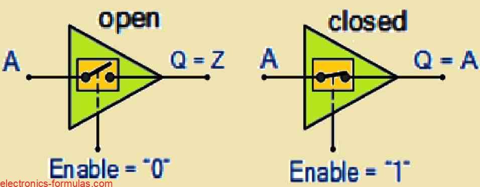
A tri-state buffer is a device that allows us to manage three possible output states, which are logic “0,” logic “1,” and a high-impedance (Hi-Z) state. In most digital circuits you will typically see the outputs as either as low (logic “0”) or as high (logic “1”), which correspond to different voltage levels. But in the case of the Hi-Z state it is special because it lets you to effectively disconnect the buffer’s output from the circuit. In this state, the buffer does not drive any voltage or draw current, so it behaves as if it is not connected to the circuit, allowing the other components to control the output without any interference.
We call the above state a “tri-state” buffer because it gives us three distinct output states: logic “0,” logic “1,” and Hi-Z. The Hi-Z state is important when we need multiple devices to share the same data bus or signal line. By placing one buffer in the Hi-Z state, we allow another device to take control of the line, which avoids conflicts because in this situation only one device drives the bus at a time, while the others remain in Hi-Z mode.
The tri-state buffer works depending on the input logic status of an enable control signal. If you apply an active-high configuration, then the buffer will produce an output which is either logic “0” or logic “1” when the “enable” control signal is high. When the control signal is switched to low, then the buffer turns into the Hi-Z state. Oppositely suppose if we use an active-low configuration, then the buffer is enabled when the control signal is low, and in this situation it enters the Hi-Z state when the signal is high.
There are actually four different types of tri-state buffers to choose from. Some of them provides us with a non-inverted output, meaning the logic level at the input is passed directly to the output when we enable the logic gate, while other types give us an inverted output, where the input is flipped or inverted. Depending on how we want it to work, we may use buffers controlled by either active-high or active-low signals which determine when the buffer is active and when it enters the high-impedance state.
Symbol and Truth Table of an Active “HIGH” Tri-state Buffer
Symbol

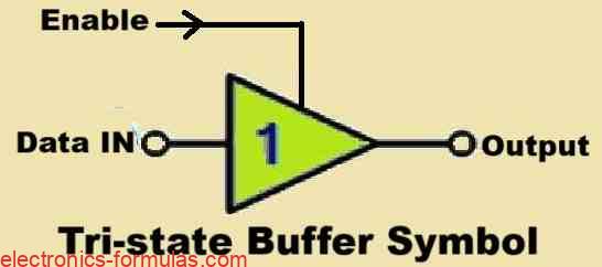
Truth Table
| Enable | IN | OUT |
| 0 | 0 | Hi-Z |
| 0 | 1 | Hi-Z |
| 1 | 0 | 0 |
| 1 | 1 | 1 |
We can read the above as Output = Input if Enable is equal to “1”
When we use an active-high tri-state buffer, for example lets say the 74LS241 octal buffer, it becomes activated when we apply a logic level “1” to its enable control line. In this state the data is allowed to pass from its input to its output, which means that the buffer is functioning and it is transmitting the input signal. However when we apply a logic level “0” to the enable line, the buffer becomes disabled, and the output enters a high-impedance (Hi-Z) state. In this Hi-Z state, the output is electrically disconnected from the circuit, so no data is transmitted, and the buffer doesn’t draw any current from the supply.
Besides the standard non-inverting configuration, in which the input signal is passed through unchanged, we can also use an active-high tri-state buffer that inverts the input signal. This means that when it is “enabled”, the output will be the logical opposite of the input. Exactly similar to the non-inverting version, when the enable control line is at logic “0,” the buffer enters the Hi-Z state, which disconnects the output regardless of whether the input is inverted or not.
The above feature gives us the flexibility in how we can control signals, which in turn allows us to choose between direct and inverted outputs while still benefiting from the tri-state functionality, which ensures that the buffer can be effectively “turned off” when it is not needed in the circuit.
Symbol and Truth Table of Active “HIGH” Inverting Tri-state Buffer
Symbol

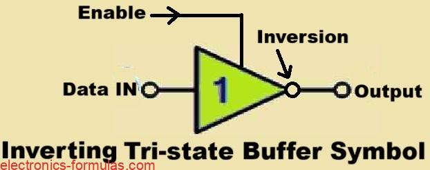
Truth Table
| Enable | IN | OUT |
| 0 | 0 | Hi-Z |
| 0 | 1 | Hi-Z |
| 1 | 0 | 1 |
| 1 | 1 | 0 |
You can Read it as Output = Inverted Input if Enable equals “1”
When we use an active-high inverting tri-state buffer, for example the 74LS240 octal buffer, it becomes active when we apply a logic level “1” to its enable control line. In this state, the data from the input is passed through to the output but it gets inverted, meaning the output is the complement of the input signal. For example suppose if we input a logic “0,” then the buffer outputs a logic “1,” and vice versa.
However suppose if we apply a logic level “0” to the enable line, then the buffer’s output is disabled, and it enters a high-impedance (Hi-Z) state, wherein the output gets electrically disconnected from the rest of the circuit, so the buffer does not create any interference with the signals on the shared line or draw any current.
We can also implement the same tri-state buffers using an active-low enable input as shown below:
Symbol and Truth Table of Active “LOW” Tri-state Buffer
Symbol

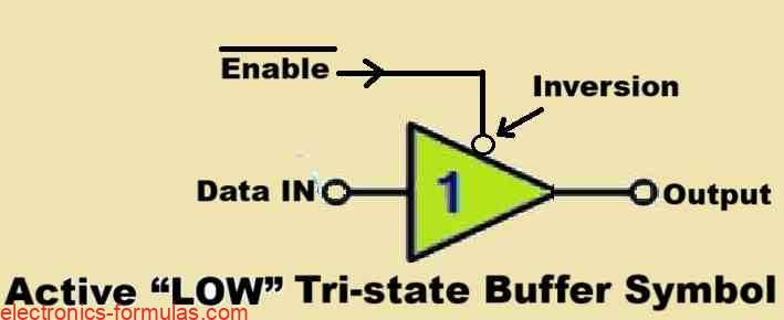
Truth Table
| Enable | IN | OUT |
| 0 | 0 | 0 |
| 0 | 1 | 1 |
| 1 | 0 | Hi-Z |
| 1 | 1 | Hi-Z |
Symbol and Truth table of Active “LOW” Inverting Tri-state Buffer
Symbol

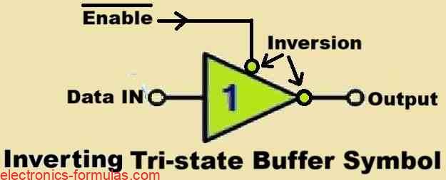
Truth Table
| Enable | IN | OUT |
| 0 | 0 | 1 |
| 0 | 1 | 0 |
| 1 | 0 | Hi-Z |
| 1 | 1 | Hi-Z |
When we use an active-low inverting tri-state buffer, we find that its behavior is just the opposite of the active-high version. Here the buffer is enabled when we apply a logic level “0” to its enable control line, and then the buffer takes the input data and inverts it, so that the output becomes the complement of the input. For example, if we input a logic “1,” the output will be a logic “0,” and vice versa.
But suppose if we apply a logic level “1” to the enable line, then now the buffer becomes disabled, and its output enters a high-impedance (Hi-Z) state, and because of this its output gets electrically disconnected from the rest of the circuit, just as as we saw in our active-high version.
How Tri-state Buffer Control Works
So far we have observed that buffers can be used to amplify voltage or current within digital circuits and also reverse the input signal. Moreover we have also noted that buffers can come in a tri-state form, allowing the output to be simply turned off and presenting a high impedance state (Hi-Z), which acts like an open circuit.
Tri-state buffers play a very important role in electronic and microprocessor designs because it allows multiple logic components to share the same line or bus without risking damage or data corruption. Let’s say, for instance, imagine we have a data bus that links together memory, peripherals, input/output devices, or a CPU, where each of these components can simultaneously send or receive data over this shared bus, potentially giving rise to conflicts.
Such conflicts arise when different components attempt to drive the bus to different logic levels, so if one component tries to set the bus to a high state while another sets it to a low state, and this can create a short circuit which may damage the components and result in a data loss.
We can transmit data across these buses either one bit at a time (serially) or multiple bits simultaneously (in parallel). In microprocessor systems we can connect several tri-state buffers to the same data bus so that it allows for effective data management without causing damage or data loss.
Tri-state Digital Buffer Data Bus Control

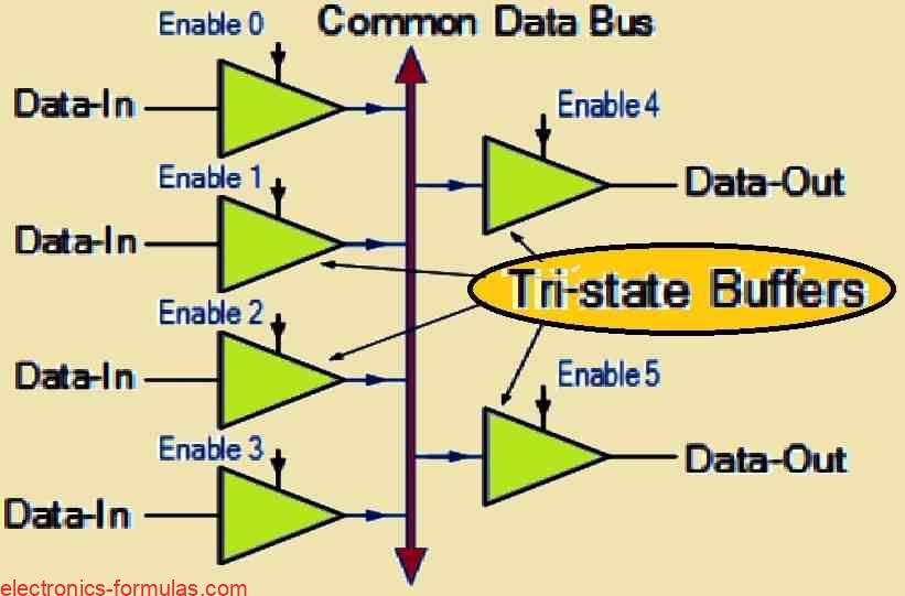
Thus we now realize that Tri-state buffers can be used to segregate devices and circuits from each other and the data bus. When we link the outputs of many Tri-state Buffers together, we may use decoders to ensure that only one set of Tri-state Buffers is active at any one moment, while the others are in their high impedance condition. This is an example of tri-state buffers coupled to a four-wire data bus.
Tri-state Digital Buffer Control

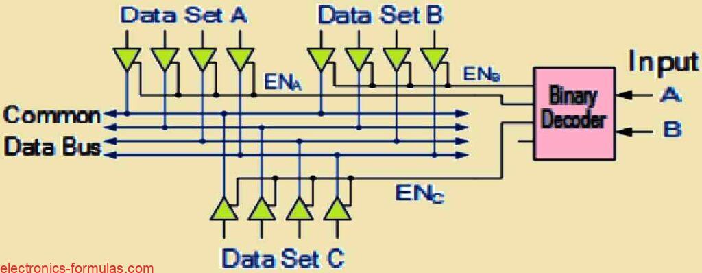
Let us consider a basic example of how a binary decoder can control multiple tri-state buffers. Here the decoder acts as a selector, which chooses the appropriate output based on its binary input, allowing us to pass only one set of data (either a logic “1” or logic “0”) onto the bus at a time. All other tri-state outputs connected to the same bus lines are disabled and are placed in their high impedance (Hi-Z) state.
In the case of data set “A,” we can transfer data to the common bus only when an active HIGH signal is applied to the tri-state buffers via the Enable line (ENA). Otherwise the data set remains in a high impedance state, which effectively isolates it from the data bus.
Similarly the data set “B” can only pass data to the bus when an enable signal is applied via ENB.
One classic example of tri-state buffers connected together to control data sets is the TTL 74244 Octal Buffer.
If needed you can also connect Tri-state Buffers “back-to-back” to create a Bi-directional Buffer circuit. In In this configuration we connect an “active-high buffer” in parallel but in reverse with an “active-low buffer,” where the “enable” control input acts as a directional control signal. This enable control allows data to be both read “from” and transmitted “to” the same data bus wire. The TTL 74245 is a tri-state buffer with bi-directional switching capability that we can implement for this type of application.
Remember, a Tri-state buffer is a non-inverting device which provides an output (identical to its input) only when the Enable (EN) pin is HIGH, or else the output goes into its high impedance (Hi-Z) state. We can mostly use the Tri-state outputs in many integrated circuits and digital systems and not just in dedicated tri-state buffers.
Both, the digital buffers and the tri-state buffer gates can be used to amplify voltage or current. This feature allows them to drive higher loads, such as relays, lamps, or power transistors, compared to conventional logic gates which are not capable of driving high current loads directly. Additionally, these buffers can also provide electrical isolation between two or more circuits.
If needed, you can make a data bus simply by connecting multiple tri-state devices together. As long as you select only one device at a time you can effectively avoid potential conflicts. Through Tri-state buses we can enable several digital devices to transfer input and output data on the same data bus using I/O signals and address decoding.
Tri-state Buffers can be commonly purchased from the market in an integrated package of quad, hex or octal buffer/drivers in both uni-directional and bi-directional forms. Among them the more common types are the TTL 74240, the TTL 74244 and the TTL 74245 as illustrated in the following table:
| Type | Device |
|---|---|
| TTL Logic | 74LS07 Hex Non-inverting Buffer |
| TTL Logic | 74LS17 Hex Buffer/Driver |
| TTL Logic | 74LS244 Octal Buffer/Line Driver |
| TTL Logic | 74LS245 Octal Bi-directional Buffer |
| CMOS Logic | CD4050 Hex Non-inverting Buffer |
| CMOS Logic | CD4503 Hex Tri-state Buffer |
| CMOS Logic | HEF40244 Tri-state Octal Buffer |
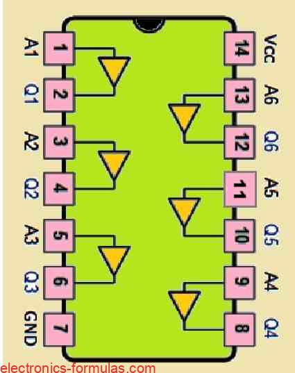
Pinout Details of a Common 74LS07 Digital Buffer

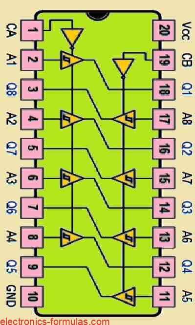
Pinout Details of a Common 74LS244 Octal Tri-state Buffer

References: What is the purpose of a buffer gate?