So both Class B amplifier and Class AB amplifier types are having this special output stage which we call push-pull type right? And in this output section we always got two power transistors or maybe sometimes two FETs also that are joined or arranged in one special manner so that these two can take the full 360 degree input waveform and then rebuild that same thing at the output side. Now whether this output is having distortion or not that will depend on many other things but mainly this is how the output is reconstructed.
An Amplifier’s Main Job
Now what we know is for any amplifier the main job is very simple — just take the small signal at the input and then increase that same signal in size so that we can drive some load with it maybe a speaker or any other device. But this amplification must be such that output still follows input shape only the size is big.
We already saw that the total power given to the load by the amplifier we calculate that by multiplying output voltage with output current which is written like P = V * I. But the input power that the amplifier eats from the power supply that is also a multiplication of DC voltage and DC current which it takes from the power source.
We already know that Class A amplifier gives good amplification because in this type the output transistor is conducting current for full 100 percent time of the input cycle. But then we also know that this type is very poor in efficiency. Why? Because even though it gives nice clean amplification it wastes a lot of power and most of the input power becomes heat not useful output. So the efficiency is less than 50 percent which is not so great.
Class B Amplifier Crossover Distortion
So what we can do is we take this same Class A idea and then we change the circuit a little to work in Class B mode. In Class B we use two transistors again but here each transistor will conduct only for half time — that is 180 degrees of the waveform. So one transistor will work for one half and other for second half. This way current is flowing in each transistor only for 50 percent time.
The good thing here is that the conversion from DC to AC becomes much better and we get around 75 percent efficiency which is very good compared to Class A. But the bad part is we get this unwanted thing called crossover distortion. This distortion happens around the zero crossing point of the waveform and it can make the audio or signal very dirty or noisy and that is not good in many applications.
So now to solve this issue we do something clever. We make a new kind of amplifier which is a mix of Class A and Class B and this new one is called Class AB amplifier. This one tries to take the best parts from both the old ones — it keeps the good efficiency of Class B and also takes the low distortion from Class A and mixes them in such a way that we get a balanced performance.
High efficiency and Low distortion
Now speaking technically, Class AB is not a completely different class, it is more like a combination or blend. But still many engineers treat it like a separate type. So in Class AB amplifier the output stage is specially made in such a way that it takes both benefits — high efficiency and low distortion — and also reduces the bad parts that we saw in Class A and B.
Pre-biasing
Like we already said above, Class AB is just like Class A and Class B working together. So when we are using it for low power signals then both the transistors will conduct together for that small part of signal just like in Class A. But if the signal becomes bigger and current demand goes high then the amplifier automatically moves more into Class B type and behaves like that. So by adjusting the biasing of the transistors properly we make this Class AB action happen. This is called pre-biasing and this small current bias is added to both transistors so that they are already slightly ON and never go completely OFF which removes the crossover distortion.
Now depending on how much load current we are giving and how we have set this pre-bias each transistor in the output stage can conduct somewhere between 180 degrees and 360 degrees. And because of this flexibility we say the amplifier is working in Class AB region.
OK then first let us check and compare how the output signals look for different amplifier classes. This will help us understand how these amplifiers behave practically.
Comparing the Different Classes of Audio Amplifiers
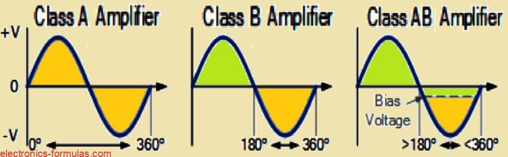
The amplifier classes have always been outlined as follows.
Class A: The single output transistor of the amplifier operates over the whole 360-degree cycle of the input waveform.
Class B: Only half of the input waveform, or 180 degrees, is conducted by the amplifier’s two output transistors.
Class AB: The two output transistors of the amplifier conduct in the range of 180° to 360° of the input waveform.
How Class A Amplifier Works
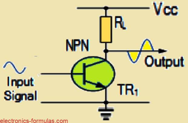
So in Class A amplifier working, what we do first is, we set the Q-point of the switching transistor — that is the quiescent point — somewhere very near to the middle part of the output characteristic load line. We do this because we want the transistor to stay fully inside the linear region during the full time of operation. That means the transistor is not going into cutoff or saturation but stays always in the active area. Because of this setup, the transistor keeps conducting current for full 360 degrees of the input signal cycle. So that way, the output we get is showing the full waveform shape same like input signal from start to end without any clipping or missing part.
The main good thing or main advantage we get from this Class A amplifier is that whatever signal we are feeding at the input side, we get almost same signal at the output side but only in bigger size or power. This makes sure that the output is very clean and almost not distorted and this is what we always want in audio or signal amplifiers. But even though the waveform is very clean and faithful to the input, still we have to face a big drawback.
That drawback is the efficiency problem. Because in this Class A setup, we always keep the transistor sitting in the center of the load line, right? So for that to happen, we need to pass a constant DC quiescent current through the switching transistor all the time. And that current keeps flowing even when there is no input signal present. So the amplifier keeps wasting power as heat even when it is doing nothing, and that makes the efficiency very low, usually lower than 50 percent.
How Class B Amplifier Works
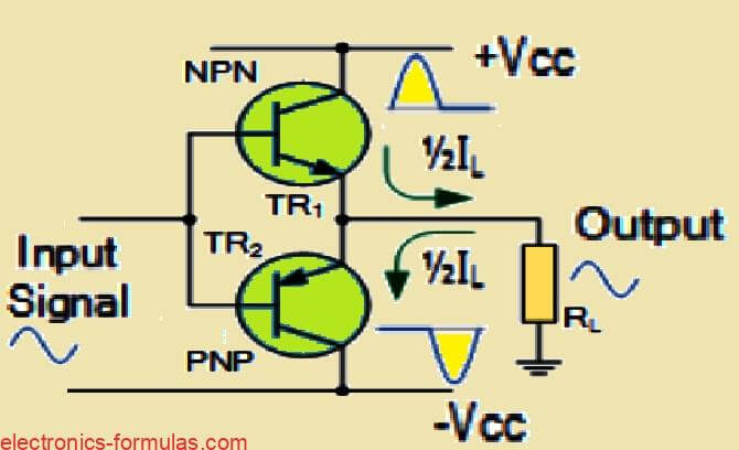
So when we are working with a Class B amplifier, what we normally do is we take two switching transistors which are complementary to each other — like one is NPN and other one is PNP type. Then we fix the Q-point or what we call the biasing point of each transistor right at the cut-off level. That means both these transistors are completely OFF when no signal is coming in.
So this setup makes one transistor turn ON and amplify the signal only during one half of the input waveform cycle. And then the second transistor takes care of the other half cycle of the input signal. Like one works for positive half and the other one works for negative half. Then after both halves are separately amplified, these are joined or merged together at the load side. So this gives us one full cycle at the output.
Now this whole arrangement with two opposite-type transistors working in turns like a team is called push-pull configuration.
Now because we are keeping the biasing at the cut-off point, that means when no input signal is applied, both the transistors are sitting totally OFF. So in that quiet condition, the quiescent current becomes zero. That means no DC current is flowing through the transistors when the amplifier is idle. So there is no power loss or heating happening in that silent state. Because of this, we get much higher efficiency compared to Class A amplifier, which wastes a lot of power even when idle. So that is a big plus point for Class B.
But still everything is not perfect here. There is one big problem. Since each transistor in Class B is designed to conduct current only during one half of the waveform so the output waveform does not fully match or follow the input signal with perfection. So that mismatch causes some amount of distortion. And this distortion is mainly happening at the zero-crossing point — that point where one transistor stops working and other one starts. So the switching between the two transistors is not smooth and that creates a small gap or glitch in the output waveform. This type of distortion is called cross-over distortion. It happens because of the little dead zone between the “OFF” state of one transistor and the “ON” state of the other.
Now to solve this cross-over distortion issue, we can do one small trick. We can slightly shift the biasing point of both transistors a little bit above the exact cut-off level. But we must be careful — we do not push it too high. We keep it still much lower than the center Q-point of Class A amplifier. So by doing this, what happens is both transistors stay just slightly ON even when the input signal is very small or zero. This way, the transition at the zero-crossing point becomes smoother and the distortion almost goes away.
So we end up creating a special type of amplifier which is a mix between Class A and Class B — and we call it Class AB amplifier. The main target of Class AB amplifier is to keep the basic structure of Class B same, but still make the output signal more clean and linear by slightly pre-biasing each transistor just above the threshold. That way we enjoy the good efficiency of Class B and also get less distortion like in Class A.
How to do Biasing for a Class AB Amplifier Circuit
Now let us see how we can do the biasing for a Class AB amplifier. That means how we can adjust the working point or Q-point of the transistors in such a way that we get the Class AB behavior. So what we normally do is, we start with a normal Class B push-pull amplifier stage — where we have two complementary transistors working alternately — and then we change it slightly by applying a small bias to both of the switching transistors. This small bias is applied even when there is no input signal coming in. That means, even in idle condition, we are making sure that both the transistors are not sitting fully OFF, but they are just slightly ON.
Now this small biasing makes both transistors conduct together at the same time, but only during a very small portion of the waveform. So instead of each transistor conducting for exactly 50% of the waveform like in Class B, in Class AB they conduct a little bit more than 50%, but still less than 100%. So they slightly overlap in conduction. That overlapping helps to remove the problem we saw earlier in Class B.
We remember in Class B amplifier, we had this issue — that crossover distortion. That problem happened because of a small voltage dead band of around 0.6 to 0.7 volts, which is equal to one forward voltage drop of a silicon diode. So because of that dead band, the output waveform had a small gap near the zero crossing.
But when we add this proper biasing in Class AB, that dead band becomes very small or even goes away completely. So we can say this crossover distortion is greatly reduced just by doing the right biasing.
So how do we do this pre-biasing practically? There are many ways for that. One method is to use a preset voltage bias, where we apply a fixed small voltage across the transistor bases. Or we can make a voltage divider circuit using two resistors to set the bias. Or even we can use a series of diodes connected in a row — like maybe two or three diodes — to produce a small fixed voltage drop which we feed to the transistor bases. All these methods help us to push the transistor bias point just above the cut-off level so that both transistors stay slightly conducting and remove that ugly distortion.
How to do Voltage Biasing for Class AB Amplifier Circuits
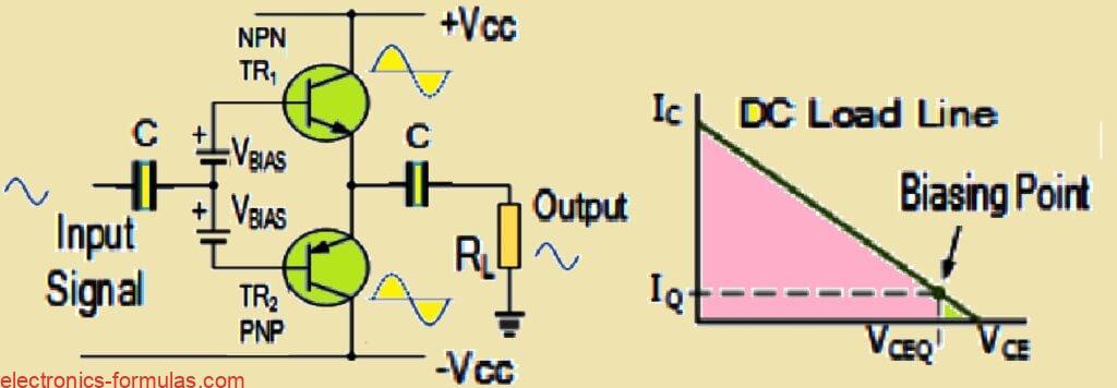
So now in this Class AB amplifier stage, the way we are doing the biasing of the transistors is by applying one proper fixed bias voltage to the bases of both transistors TR1 and TR2. That voltage is already set in such a way that it keeps both the transistors just a little bit ON all the time. Then because of this, there is a small region in the signal cycle where both transistors are conducting together.
So what happens is, the small quiescent collector current flowing through TR1 adds together with the small quiescent collector current flowing through TR2. And both these small currents combine and go into the load.
Then when the input signal starts to go in the positive direction, the voltage at the base of TR1 also starts increasing. So TR1 responds by producing one positive output voltage, almost similar to that input change. This causes the collector current in TR1 to increase more, and it begins to source more current into the load resistor RL. But because we had already fixed the voltage between the base of TR1 and TR2, that voltage stays constant. So when TR1 starts conducting more during positive half cycle, at the same time TR2 has to reduce its conduction by the same amount. That happens automatically because of the fixed bias.
So then as the signal goes more and more positive, TR2 keeps decreasing its conduction and finally goes OFF completely. And then TR1 alone remains forward biased and fully active, and it alone supplies all the current to the load during that time. So TR1 is doing the full job for the positive half.
During the negative half of the input signal, just the opposite thing happens. The input voltage starts going negative, and because of that, TR2 now becomes more forward biased and it starts conducting more. It sinks the current from the load now. And at the same time TR1 starts going into OFF condition slowly. So finally TR1 turns off completely and TR2 alone handles the negative half by sinking all the current from the load.
So then we can clearly see one important thing — when the input voltage VIN is exactly zero, that time both TR1 and TR2 are slightly conducting together, just because of the voltage biasing we have applied. But when the input voltage starts moving either towards positive or towards negative, then one of the two transistors takes control and conducts more. One of them starts sourcing or sinking the load current, depending on whether the input is positive or negative.
So when we talk about the switching between the two transistors in a Class AB amplifier, we see that this switching happens almost immediately and also in a very smooth manner. That means one transistor slowly goes OFF while the other one slowly comes ON, without any harsh break in between. Because of this smooth transition, the crossover distortion that we normally get in Class B amplifier is reduced a lot. So the waveform near zero crossing becomes much cleaner.
But still we need to be a little careful. If we do the biasing in a wrong way, or if the biasing is not accurate, then this switching will not be smooth anymore. And then we can get some sharp crossover distortion spikes at the point where one transistor is turning OFF and the other is turning ON. So bad biasing can make the output waveform distorted again, which we do not want.
Now to solve this, we normally use a fixed bias voltage. This fixed voltage makes sure that both transistors can conduct for a bit more than half of the input waveform cycle. That is why we call it Class AB operation, because now each transistor is working more than 180 degrees, but less than full 360 degrees.
But let us think practically. If we say we will use some extra batteries to apply fixed biasing voltage to the transistors, then that is not very practical in a real amplifier design. We cannot put extra batteries just to bias the output stage. That would be messy and not useful for long term operation.
So then what we do is, we go for a very simple and easy method. One method that works really well is to use a resistive voltage divider network. We connect this across the same single DC supply that we already have. This voltage divider gives us two stable bias voltages. And these voltages can be set in such a way that the Q-point of both the transistors comes close to their cut-off point. This helps us to achieve the Class AB working condition without adding anything extra like batteries.
How to do Resistive Divider Biasing in Amplifier Circuits
Now when electric current flows through any resistor, then we know from Ohm’s law that a voltage drop happens across that resistor. So this voltage drop depends on the resistance value and the current passing through it.
If we take two or more resistors and connect them in series across a power supply, then we can build something called a voltage divider network. This divider network helps us to get different fixed voltages that we can use as per our circuit’s needs.
Now this basic voltage divider setup is almost same like the one we already discussed earlier, where we used resistors for biasing the bases of the transistors TR1 and TR2. These two transistors work in opposite halves of the input waveform. That means when the input voltage, VIN, becomes positive, then TR1 starts conducting. And when the input voltage goes negative, then TR2 starts conducting. So they handle different sides of the waveform.
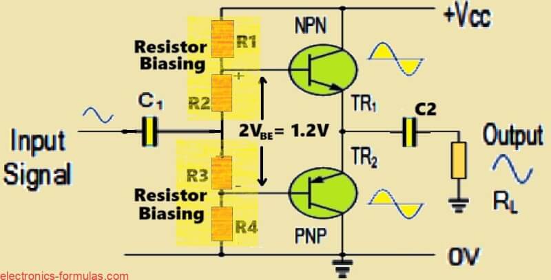
Now here in this circuit, we are using four resistors, which are R1, R2, R3, and R4. All these resistors are connected across the supply voltage Vcc, and they create the required resistive biasing network. The resistors R1 and R4 are specially selected in such a way that they help to set the Q-point of the transistors just a little above the cut-off level. We do this by making sure that the VBE value of each transistor is around 0.6V, because that is the forward voltage needed for silicon transistors.
So with this setup, the voltage at the base of TR1 becomes around +0.6V, and the voltage at the base of TR2 becomes around –0.6V. Then the total voltage drop across the two middle resistors, R2 and R3, becomes close to 1.2V. This is just slightly below the voltage that would fully switch ON the transistors. So we are keeping both transistors just above the cut-off point but not fully conducting. That way we get the quiescent collector current, ICQ, almost equal to zero. So the amplifier stays in its ready state without wasting power when there is no input signal.
Also if we look at the arrangement of these two transistors, they are actually placed in series across the power supply. Because of that, the voltage across the collector and emitter of each transistor, which is called VCEQ, becomes roughly half of the total Vcc supply voltage. So both transistors share the supply voltage equally when idle.
Now even though this resistive biasing method looks good and works fine in theory, we have to know one important thing. The collector current of a transistor is very much sensitive to small changes in its base-emitter voltage, VBE. Also in real life, the two complementary transistors (NPN and PNP) may have slightly different cut-off points. So that makes it difficult to choose the exact resistor values for the voltage divider network that can give perfect Q-point.
But then we do have a nice and simple trick to fix this issue. We can use an adjustable resistor, also called a variable resistor or preset. This preset can be used in the voltage divider so we can fine-tune the biasing voltage. That way we can precisely set the correct Q-point that we want for Class AB amplifier operation.
How to Implement Adjustable Biasing for Amplifier Circuits
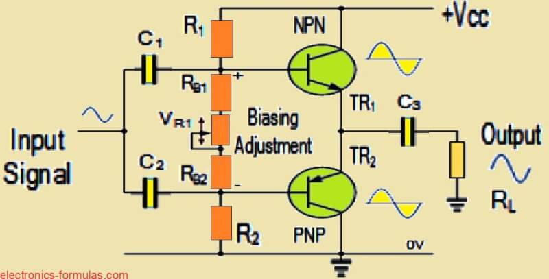
Now here what we do is we use one adjustable resistor which we also normally call a potentiometer and this is used for setting the proper bias level for both the transistors,TR1 and TR2, so that they just start conducting or we can say they are right on the edge of conduction.
So in this circuit the biasing path is made using three parts: one resistor RB1, then the potentiometer VR1, and then another resistor RB2. This whole setup makes sure that both TR1 and TR2 are biased properly and equally, and also that there is no quiescent current flowing into the load when there is no signal.
Then we give the input signal from the outside through two capacitors, which are C1 and C2. These capacitors help to superimpose the input signal on top of the DC bias voltage. After this, the combined signal reaches the bases of both transistors. But here we must remember one thing—both transistors get the same signal, with same frequency and same amplitude, because both are coming from the same input source, which is VIN. So the only difference in action comes from their polarity and the input phase.
So the biggest benefit we get from using this adjustable biasing system is that now we do not have to worry too much about the matching of the complementary transistors. That means even if TR1 and TR2 are not perfectly matched in their electrical properties still we can balance the whole thing by adjusting the potentiometer. Also we do not need to find perfect resistor ratio in the voltage divider network. We can just tweak the preset, and compensate for everything.
But now comes one problem that we must not ignore. Since resistors are passive components, they do not amplify or control power actively, but instead they dissipate power as heat. So this means that when we are using resistive biasing method in our Class AB amplifier, whether it is fixed bias or adjustable bias, the performance can become very sensitive to changes in temperatures. Even small changes in temperature can cause resistors or transistors to change their characteristics a little bit and this can give rise to unwanted changes in the quiescent collector current which can mess up the performance.
So to solve this heating and temperature issue in a better way, we can go for another method. One very perfect solution is to change those resistors with diodes. This is called diode biasing and it helps to keep the bias stable even when the temperature goes up or down.
How to Implement Diode Biasing in Amplifier Circuits
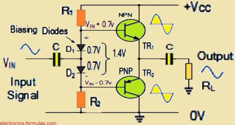
So what happens is, when we try to use biasing resistors, we may feel like we are solving the temperature trouble but actually that is not fully true. We still can get affected by temperature changes. But then one really smart way to fix the problem of base-emitter voltage (VBE) changing due to temperature up and down is by adding two ordinary forward-biased diodes inside the biasing setup of the amplifier. We can see this in the diagram if we check properly.
Now in this setup we pass one small and constant current through a series path which includes R1 then D1 then D2 then R2. Because of this setup, the voltage drop becomes equal and balanced on both sides of the input. And when we do not apply any input signal at all, then the point between those two diodes stays at zero volts. But as soon as current flows through this path, the diodes each drop about 0.7V, because they are forward biased, and this voltage is now sent to the base-emitter junctions of the switching transistors.
So the diode voltage drop biases the base of TR1 to about plus 0.7V and the base of TR2 to around minus 0.7V. That gives us a total of 1.4 volts between the two transistor bases. This is good because now both the transistors are pushed just above their cutoff point, which is perfect for Class AB working condition.
But when the temperature goes up then not only the transistors but also the diodes which we place very close to the transistors, also get warm. And when that temperature rises, then the voltage across the PN junction of the diodes starts falling down. This dropping voltage causes some of the base current of the transistor to reduce or divert and this actually helps to stabilize the collector current. So we are getting some kind of self-regulation here.
Now if we manage to use diodes that are electrically very close or similar to the base-emitter junctions of the transistors, then we can achieve something called a current mirror effect. What that means is, the current that is going through the diodes becomes almost equal to the current going into the transistors. And because of this, the circuit behaves like a mirror for the current which keeps everything balanced even when temperature keeps changing. That is how we can maintain proper Class AB operation without any crossover distortion.
And in real life we do not even have to worry much. Why? Because in most modern integrated circuit amplifiers, this diode biasing trick is already built-in. The designers already put both the diodes and the switching transistors inside the same IC chip, like we see in the famous LM386 audio amplifier IC. So since they are inside the same silicon chip, they behave exactly the same even if temperature goes up or down. That helps to keep the quiescent current nicely stable across wide range of temperatures.
So when we talk about the biasing part of the output stage in a Class AB amplifier then we have to remember that it is not always fixed or standard. We have to adjust it depending on what our application is asking for. Different amplifier needs different biasing styles. So we have to set the quiescent current accordingly.
Sometimes we can set this quiescent current to zero, just like what we do in a Class B amplifier because this helps to save power and reduce unwanted power consumption when there is no input signal. But in other cases if we want to get real Class AB working, then we must allow a small amount of quiescent current to flow even when the input is zero. This small current helps in reducing the crossover distortion and gives us a cleaner output, with less signal error.
Now in all these Class AB amplifier circuits which we discussed earlier, we saw that the input signal goes straight to the bases of the switching transistors. And to make that happen, we use coupling capacitors which join the input source with the transistor bases without disturbing the DC biasing.
But still we can improve this circuit even more. That means that we can make the output stage of the Class AB amplifier work even better. So how do we do that? Then the answer is by adding a simple driver stage before the output transistors.
This driver stage is usually designed in common-emitter configuration, and it works like a current booster and also improves the overall gain and control. So if we place this common-emitter driver stage before the Class AB output stage, then the whole amplifier becomes more stable, more linear and gives better sound or output quality.
And we can see this enhancement clearly if we look at the diagram where this improvement is shown. So basically, we start from a simple Class AB stage then we upgrade it by putting one more transistor stage in front of it, and that is the common-emitter driver which pushes the output stage in a smoother way.
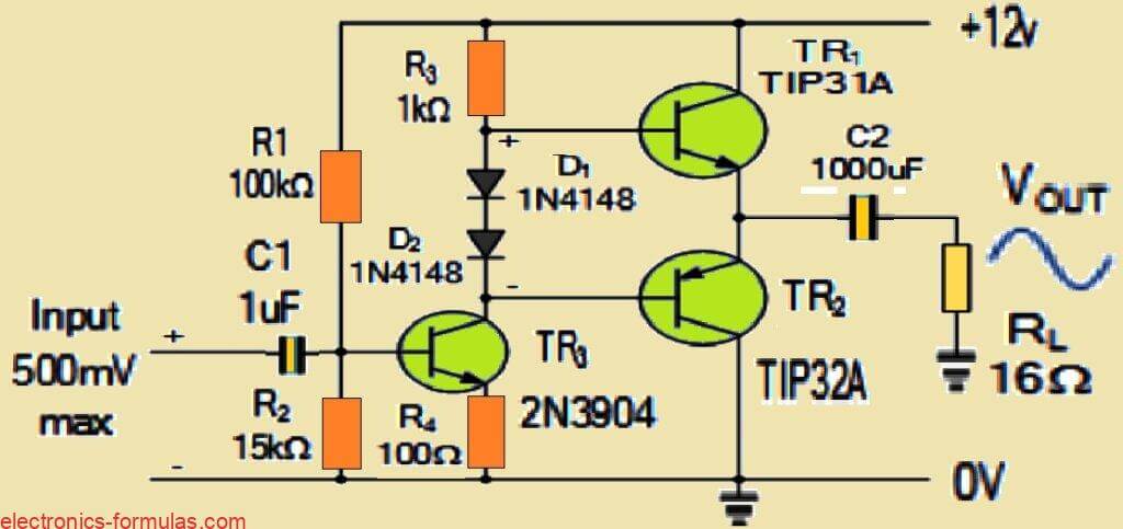
Designing a Class AB Amplifier Driver Stage Circuit
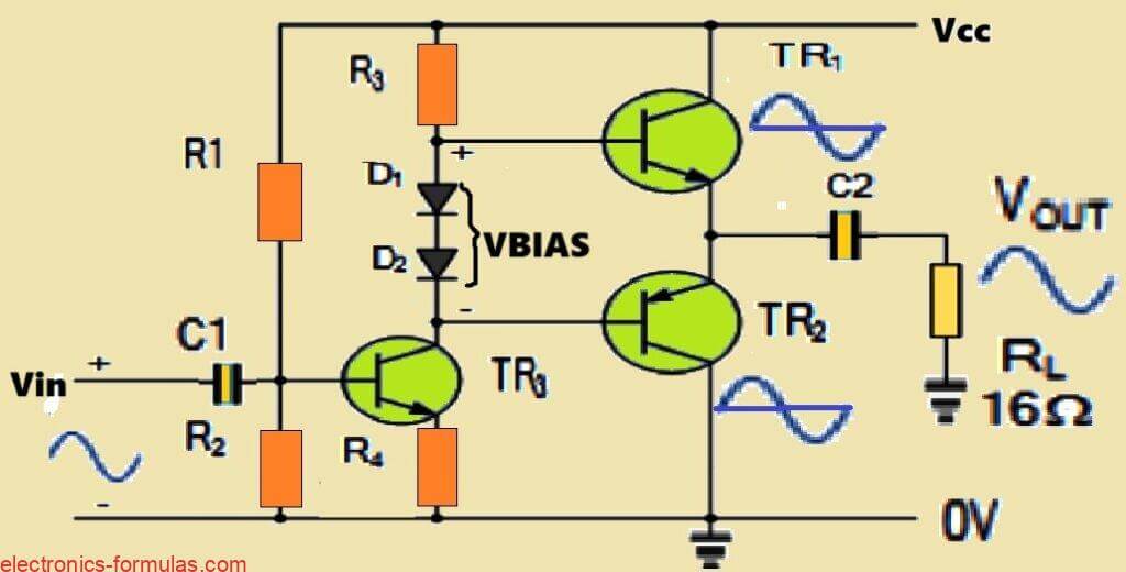
So in this circuit what we are seeing is that transistor TR3 is doing a very important job. It is working like a current source and it is giving the correct amount of DC biasing current which is needed to flow through the diodes in the circuit. Because of this setup, we get a quiescent output voltage that is around Vcc divided by 2, or simply we can say Vcc/2.
Now when we send the input signal into the base of this TR3 transistor then this transistor starts working like a small amplifier stage and it begins to drive the bases of TR1 and TR2. That means it starts controlling both output transistors depending on the input cycle.
So during the positive half part of the input waveform TR1 turns ON and TR2 stays OFF. Then during the negative half, the reverse happens — TR2 turns ON and TR1 turns OFF. So the working style or pattern is same like what we already discussed before in Class B or Class AB.
As we already know from electronics basics, there are many different ways to make or build the output stage in power amplifiers. That means we can modify the design we can adjust the components, and we can change the configuration to suit our need but all of them are based on some basic amplifier output circuit.
Now the main job of a power amplifier is always to give a strong output power to the connected load. This power must have enough voltage and current so that the load can work properly. At the same time we also try to keep the efficiency of the amplifier reasonably good — so that less heat is wasted and more power goes to the load.
So to make this happen, we have two basic options. We can make the output transistor work in Class A mode or in Class B mode. Each one has its own pros and cons.
But if we want to get good efficiency and also avoid crossover distortion then one good way is to use a Class B output stage with a symmetrical design. That means we use a NPN transistor and a PNP transistor which are complementary to each other. We set both of them with a correct level of forward bias so that both transistors do not turn OFF at the same time. That is how we reduce the crossover distortion problem.
So if we do this biasing properly then this amplifier becomes what we call a Class AB amplifier — which is like a middle ground between Class A and Class B, giving us better overall performance.
And finally if you now want to build a simple working Class AB power amplifier practically then you can go ahead and construct the circuit as shown below. This basic amplifier circuit can easily deliver around 1 watt of power into a 16-ohm load, and the frequency response will cover all audio signals from about 20Hz to 20kHz.
Sources:
Leave a Reply