
The NAND (Not-AND) gate is a fundamental digital logic gate which is designed to operate using a combination of an AND gate followed by a NOT gate. This means that the output of a NAND gate is generally at a logic level “1” (high) except in one specific case wherein it only switches to a logic level “0” (low) when every one of its inputs is at a logic level “1”.
In other words if you want the output of a NAND gate to be “0”, you must make all its inputs logic high or “1”. This behavior is just the the opposite or “complementary” to that of an AND gate wherein the output is “1” only when all inputs are “1”. Therefore we can conclude that the NAND gate provides a negated or an opposite version of the AND operation.
Diagram Depicting the Equivalent of a Logic NAND Gate

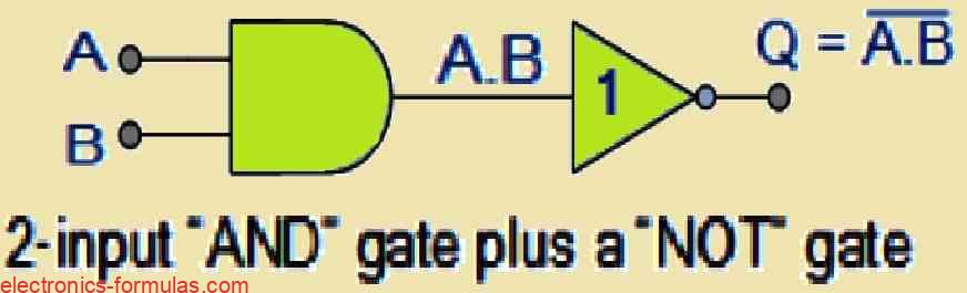
The Boolean expression for a NAND gate provides us a form of logical addition that is the inverse of the AND gate and which operates on the complements of the inputs. This expression is indicated by a dot or period (.) with an overline (‾‾) to denote the NOT operation or logical negation which gives us the Boolean expression:
A.B = Q
Therefore we can describe the function of a 2-input NAND gate in the following manner:
“If both A and B are true, then Q is false.”
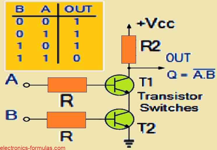
NAND Gate using a BJTs
We can easily build a transistor-based NAND gate by using Resistor-Transistor Logic (RTL), wherein resistors and transistors (BJTs) can be used to create the NAND gate’s functionality. If we take the example of a simple 2-input NAND gate made with the RTL, we find that the two inputs are connected directly to the bases of two transistors.
If you want the NAND gate output to generate an output of “1” (high) at Q, then at least one of the transistors must be “cut-off” or in the switched “off” state. This means that if both transistors are conducting (i.e., both are “on”), the output at Q will be “0” (low), but on the other hand if either one of the transistor is off, the output will be “1”.

We also get digital circuits which come with integrated NAND gates that perform this same logical function. These digital NAND gates are indicated using the same symbol which is used to indicate an AND gate, but the only difference being a small circle, known as an “inversion bubble,” which is put at the output of a NAND gate symbol.
As we learned previously, this tiny circle represents the NOT operation, indicating that the output is the inverse of the AND function.
Symbol and Truth Table of Logic “NAND” Gate with 2-input Function
Symbol

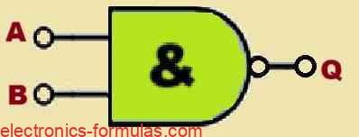
Truth Table
| B | A | Q |
| 0 | 0 | 1 |
| 0 | 1 | 1 |
| 1 | 0 | 1 |
| 1 | 1 | 0 |
Boolean Expression Q = A.B, we can read as A AND B gives NOT Q
Symbol and Truth Table of Logic “NAND” Gate with 3-input Function
Symbol
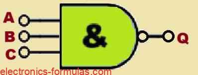
Truth Table
| C | B | A | Q |
| 0 | 0 | 0 | 1 |
| 0 | 0 | 1 | 1 |
| 0 | 1 | 0 | 1 |
| 0 | 1 | 1 | 1 |
| 1 | 0 | 0 | 1 |
| 1 | 0 | 1 | 1 |
| 1 | 1 | 0 | 1 |
| 1 | 1 | 1 | 0 |
Boolean Expression Q = A.B.C, we can read this as A AND B AND C gives NOT Q
Just like the AND function we discussed earlier, the NAND function can handle multiple inputs. You can find NAND gate integrated circuits (ICs) on the market which come with 2, 3, or 4 inputs, but if you are interested to have more inputs than these ICs provide, then you can simply connect multiple NAND gates in series, or “cascade” them in order to create a circuit that accommodates more inputs, as desired by you.
Understanding Logic “NAND” Gate with 4-input Function

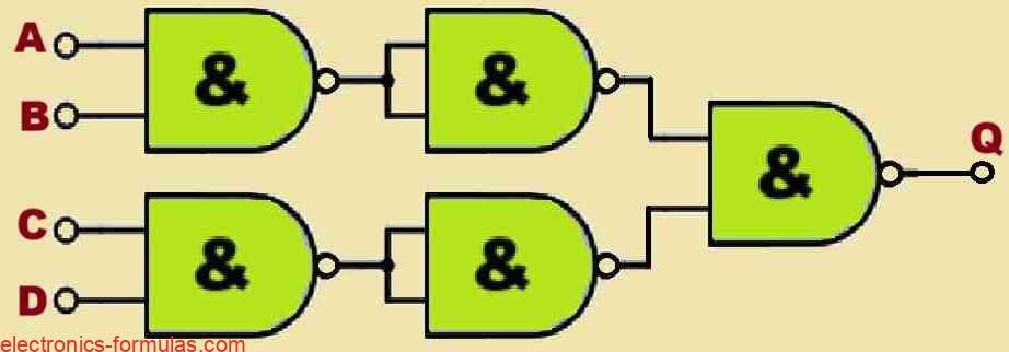
For a 4-input NAND gate, we can write its Boolean expression in the following form:
Q = A.B.C.D
Now suppose if you need an odd number of inputs than just 4, then you can simply hook up any extra unused inputs directly with the power supply through “Pull-up” resistors to make them HIGH.
The NAND gate function is also sometimes referred to as the Sheffer Stroke Function and this is indicated by a vertical bar or an upward arrow, so you might also sometimes see the NAND function written as such as, A NAND B = A|B or A↑B.
Why NAND Gate is a “Universal” Logic Gate
The NAND gate is often referred to as a “Universal” logic gate because it is incredibly versatile and one of the most commonly used types of logic gates. Also these logic gates allow us to create any other type of logic gate function as required. This means that, in practice, we can use NAND gates as the building blocks for developing most of the practical logic circuits.
By connecting NAND gates together in different combinations we are able to generate all three fundamental types of logic gates, which are AND, OR, and NOT. So just by using NAND gates only, we are able to create any of these essential logic functions which simply proves just how universal and indispensable these logic gates can be in circuit designing.
Here are some examples which show how NAND gates can be used to create other forms of logic gates.
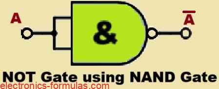
NOT Gate using NAND Gate

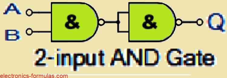
2-Input AND Gate using NAND Gates

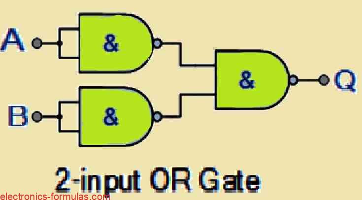
2-Input OR Gate using NAND Gates

Most common types of digital logic NAND gate IC’s which you can get readily from the market are indicated in the following table:
| Type | Part Number | Configuration |
|---|---|---|
| TTL Logic NAND Gates | 74LS00 | Quad 2-input |
| 74LS10 | Triple 3-input | |
| 74LS20 | Dual 4-input | |
| 74LS30 | Single 8-input | |
| CMOS Logic NAND Gates | CD4011 | Quad 2-input |
| CD4023 | Triple 3-input | |
| CD4012 | Dual 4-input |
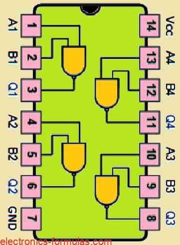
Pinout Diagram of IC 7400 which is a common Quad 2-input Logic NAND Gate

In our next Digital Logic Gates tutorial, I will comprehensively discuss about digital logic NOR Gate function which may be implemented in both TTL and CMOS logic circuits, in addition to this, I will also help you to learn its Boolean Algebra definition and truth tables.
References: NAND Gate