When we talk of PNP BJTs, they are essentially the reverse of NPN transistors in structure. Instead of having two diodes alligned in the same direction, PNP transistors have them flipped around. This forms a Positive-Negative-Positive (PNP) configuration. If you look at the symbol for a PNP transistor, you will notice that there is an arrow pointing inward. This arrow indicates the location of the emitter terminal.
Now let us get into polarities. In a PNP transistor we find the polarities are reversed compared to an NPN transistor. So instead of pushing current out through the base, a PNP transistor pulls or “sinks” current into its base. It is as if they have swapped roles with the NPN version!
The main thing to rememeber here is that PNP transistors rely on holes (the absence of electrons) as their main charge carriers. In contrast, NPN transistors use electrons as their main carriers.
How do the PNP transistors work? They can be turned ON by applying a small current at the base with a negative voltage, to control a much larger current between the emitter and collector. Simply put, for a PNP transistor to switch ON, its emitter must be more positive than both the base and the collector.
As for the construction, a PNP transistor consists of two pieces of P-type semiconductor material on either side of an N-type material. It is like having two positive sides around a negative center, as shown in the following image!
PNP BJT Internal Layout Configuration

The arrow on a transistor symbol indicates how the emitter works and shows the direction of conventional current flow.
Interestingly, PNP transistors operate similarly to NPN transistors. The key difference is that the current and voltage biasing directions are completely opposite. This reversal applies across all three configurations we covered in our first tutorial: common base, common emitter, and common collector.
So although the NPN and PNP BJT versions share similar working characteristics, we need to remember that their voltage and current polarities are totally reversed.
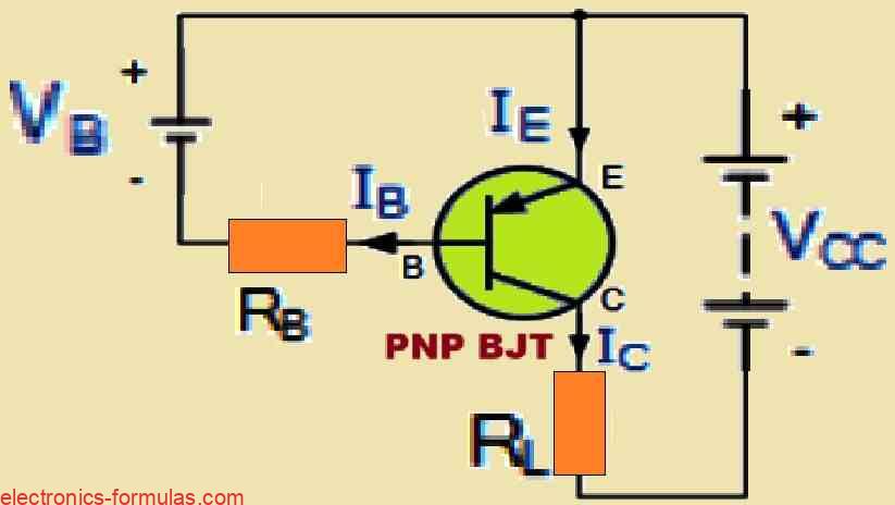
PNP BJT Connection Circuit

When we are looking at the voltage between the Base and Emitter which we call VBE, it is actually showing up as negative at the Base and positive at the Emitter.
This is because for a PNP transistor, the Base terminal is always sitting at a negative bias compared to the Emitter.
Now if we check out the Emitter supply voltage, we see that it is positive when we compare it to the Collector (that is VCE).
So, for our PNP transistor to start doing its thing and conduct, the Emitter has to be more positive than both the Base and the Collector.
When we connect our voltage sources to a PNP transistor, it looks like this: the Emitter hooks up to the supply voltage VCC, and there is also a load resistor RL at the collector terminal.
This RL resistor helps to keep the maximum current flowing through whatever device we have connected to the Collector terminal in check.
Then we have the Base voltage VB which is biased negatively compared to the Emitter. It connects to a Base resistor RB which again plays a role in limiting how much Base current can flow.
Now for us to get that Base current flowing in a PNP transistor, we need to make sure that the Base is more negative than the Emitter by about 0.7 volts if we are using a silicon type BJT, or around 0.3 volts for germanium BJTs.
The cool part is that when it comes to calculating things like Base resistor values, Base current, or Collector current, we can use the same formulas that we would use for an equivalent NPN transistor. So here’s how it goes:
IC = IE – IB,
IC = β * IB, and IB = IC/β.
When we look at the main differences between NPN and PNP transistors, the biggest thing we notice is how we need to set up their connections.
The current direction and voltage polarities are always reversed which is interesting! In this circuit, the relationship is collector current = emitter current – base current since the current flows out of the base.
Generally we can swap NPN transistors with PNP transistors in most circuits without much trouble. The only thing to keep in mind is the direction of the currents and the voltage polarities.
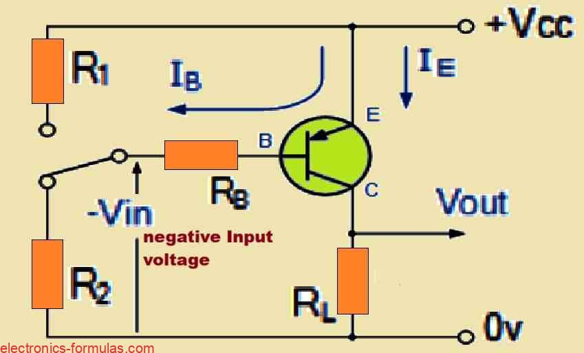
Also PNP BJTs are very useful and can work well as switches too. There is an example of a PNP transistor switch circuit below that shows just how handy they can be while operating a DC load!
Analyzing a PNP BJT Circuit

When we refer to the characteristics curves of a PNP BJT, we find that, basically, these curves look almost exactly like the ones for an equivalent NPN transistor. The big difference though, is that they are rotated by 180 degrees.
This rotation takes into account the reversed polarity of the voltages and currents in a PNP transistor. For a PNP setup, the current flows out of the base and collector which is just the opposite to how it works in an NPN transistor.
Even with this difference, we can still draw the same type of dynamic load line onto the current-voltage (I-V) curves for a PNP transistor.
This line helps us pinpoint the operating points, or “sweet spots,” for the PNP transistor, just like we would for an NPN transistor.
The Importance of PNP BJTs as Complementary Transistors to NPN BJTs
You might wonder, why even bother with PNP transistors when we have loads of NPN transistors that work perfectly as amplifiers or solid-state switches? Well, having both PNP and NPN transistors gives us more flexibility, especially when we are designing circuits for things like power amplifiers, such as Class B amplifiers.

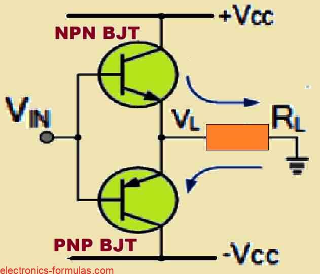
In a Class B amplifier, we use something called a “complementary” or “matched pair” setup, which involves pairing one PNP transistor with one NPN transistor in the output stage.
This combination is super useful because it helps us manage current flow more effectively in both directions. For example, in a reversible H-bridge motor control circuit, we can use this pairing to control the current so that it flows through the motor in either direction, allowing us to switch between forward and reverse motion as needed.
This way we get a smooth, balanced control over the motor in both directions which is a major advantage!
When we put together an NPN and a PNP transistor with almost identical characteristics, we call them “complementary transistors.” These transistors are like matched partners, working together with similar properties.
For example, the 2N3055 (an NPN BJT) and the 2N2955 (a PNP BJT) are great examples of complementary pairs in the world of silicon power transistors.
These two are designed to have a very close DC current gain (Beta) that only varies by about 10%, and they can handle a high collector current of many amps.
This makes them perfect for applications where we need reliable motor control or want to drive robotic systems.
In a Class B amplifier, we normally use complementary NPN and PNP transistors in the power output stage. Here is how they work: the NPN transistor handles only the positive half of the signal, while the PNP transistor takes care of the negative half.
This pairing allows the amplifier to deliver power to a load, like a speaker, in both directions with the correct impedance and power output.
As a result, the output current, which can reach several amps, is shared evenly between the two complementary transistors, giving us a smooth and balanced output. This setup is a big reason why complementary transistors are so valuable in amplifier design!
How to Identify if a BJT is a PNP Transistor
From our previous studies we know that BJTs are in essence, like two diodes hooked up back-to-back. This layout gives us an easy way to identify whether we are working with a PNP or NPN transistor, just by checking the continuity between its three main leads: the Emitter, Base, and Collector.
By using a multimeter and testing each possible pair of these leads in both directions, we end up with a total of six measurements. These tests give us a good idea regarding what type of transistor we have got based on the continuity readings, which should follow the expected values as listed below:
- Emitter-Base Terminals – Here the Emitter-Base connection should behave like a regular diode, allowing current to pass in only one direction.
- Collector-Base Terminals – Similarly, the Collector-Base junction should also act like a diode, conducting current in just one direction.
- Emitter-Collector Terminals – Unlike the previous pairs, the Emitter-Collector terminals should show no conduction at all, regardless of the direction of testing.
By following this simple guide, we can accurately figure out the BJT type PNP or NPN based on these resistance patterns.
Continuity Measurements for PNP and NPN Transistors
| Between Transistor Terminals | PNP | NPN | |
| Collector | Emitter | RHIGH | RHIGH |
| Collector | Base | RLOW | RHIGH |
| Emitter | Collector | RHIGH | RHIGH |
| Emitter | Base | RLOW | RHIGH |
| Base | Collector | RHIGH | RLOW |
| Base | Emitter | RHIGH | RLOW |
Conclusions
You can think of a PNP transistor as a device that is normally in the switched OFF condition. But here’s the trick: if we apply a small current with a negative voltage at the Base (B) relative to the Emitter (E), it will switch “ON.” This opens the gates, allowing a much larger current to flow from the Emitter to the Collector.
In other words, for a PNP transistor to conduct, the voltage at the Emitter has to be much higher than the voltage at the Collector, with both the Base and Collector needing to be more negative compared to the Emitter.
Now, coming up in our next transistor tutorial, we will learn more about a different use for these BJTs, this time, not as amplifiers, but as solid-state switches. We will dig deep into how transistors operate in their “saturation” and “cut-off” regions, which are simply the “ON” and “OFF” states.
These bipolar transistor switches are super versatile and show up in tons of applications! We use them to switch DC currents on and off, whether it is for low-power tasks like lighting up LEDs (which need only a small current at lower voltages) or more demanding jobs like powering motors and relays, which often require higher currents and voltages.
References:
When would I choose to use a PNP BJT
PNP Bipolar Junction Transistors (BJTs)
Leave a Reply