If you want to keep a bipolar transistor running smoothly, it really comes down to getting the right balance of its base current, collector voltage, and collector current.
So if we want to use a transistor as a linear amplifier, we have got to bias it properly.
Biasing basically means setting it up so it is ready to amplify signals without messing them up. If we do not bias it right the output signal gets distorted, and nobody wants that!
To get this biasing right, we need to pick the right bias resistors and load resistors. These resistors help us to control the input current and collector voltage which are so important.
Now the ideal biasing point for our transistor, whether it is NPN or PNP, is usually somewhere in the middle of its operational range. It should not be fully “ON” or fully “OFF”. We call this sweet spot the “Quiescent Operating Point” or just the “Q-point” for short.
When we bias the transistor so that the Q-point is in the middle – about halfway between cut-off and saturation – we say it is running as a Class-A amplifier.
This is cool because the output voltage can swing up and down around the Q-point without any distortion. Basically we get the full output signal for the entire 360 degrees of the input cycle.
Base Bias
When we are trying to nail down that perfect Q-point for biasing a transistor, we often use something called Base Bias. But before we learn more about the different ways we can bias a transistor, let us just take a quick peek at a basic single transistor circuit along with all its voltages and currents.
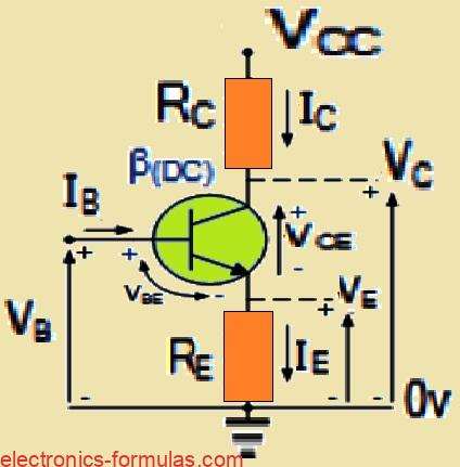
Now the whole point of the “DC Bias level” is to get the transistor’s Q-point just right by making sure its Collector current is steady and constant, even when there is no input signal messing with the transistor’s Base.
This steady or DC operating point is determined by how much DC supply voltage (Vcc) we are feeding into the circuit and also the values of any biasing resistors that are hooked up to the transistor’s Base terminal.
Since the transistor’s Base bias currents are steady DC currents, throwing in some coupling and bypass capacitors can help block any biasing currents from other transistor stages from messing up the bias conditions of the next stage.
Base bias networks can be used for Common-base, common-collector, or common-emitter transistor setups. In this explanation we are looking at the different biasing arrangements for a Common Emitter Amplifier.
Biasing a Common Emitter BJT Configuration
So when you are setting up a transistor circuit, one super common way to do it is with a self-biasing emitter-bias circuit. Basically you use a bunch of resistors to get the initial DC currents just right for the transistor—that is your IB, IC, and IE.
Now there are two main ways to bias a bipolar transistor: Beta Dependent and Beta Independent. Transistor biasing usually depends a lot on the transistor’s beta (β), so the way you bias one transistor might not work for another since their beta values could be different.
You can bias a transistor by using a single feedback resistor or a voltage divider network to get the voltage you need.
Here are five examples of how you can set up the transistor with Base bias using a single supply (Vcc).
Using Fixed Base Biasing for a BJT
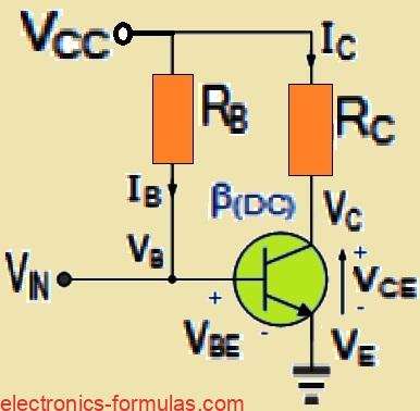
VC = VCC - (IC * RC)
VCE = VC - VE
VE = 0V
VB = VBE
IB = (VCC - VBE) / RB
IC = β(DC) * IB
IE = (IC + IB) ≅ IC
So this type of BJT biasing is called a “fixed base bias circuit”. Basically the transistors base current IB stays pretty steady for certain values of VCC which means the transistors operating point is also fixed. This setup using two resistors is how you initially set up the transistors operating region with a constant current.
Now this biasing arrangement is “beta dependent” meaning the transistors beta (beta) value affects how it operates in a steady state. So the biasing point can change a lot between transistors of the same type because their characteristics are not exactly the same.
To forward bias the transistors emitter diode you apply the necessary positive base bias voltage through a current limiting resistor RB. If you are using a typical bipolar transistor, then the forward base emitter voltage drop is about 0.7V. You can figure out the value of RB with the formula:
(VCC – VBE)/IB, where IB is IC/beta.
But with this single resistor biasing method, the biasing voltages and currents are not very stable when the transistor is running and can change quite a bit. Also the transistors operating temperature can mess up with the operating point.
Using BJT Collector Feedback Biasing
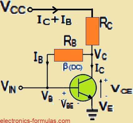
VC = VCC - RD(IC + IB)
VE = 0V
VB = VBE
IB = (VC - VB) / RB
IC = β(DC) * IB
IE = (IC + IB) ≅ IC
So this setup is called a “self biasing collector feedback configuration.” It is another one of those beta dependent biasing methods that uses two resistors to give the transistor the DC bias it needs.
What is cool about this collector to base feedback setup is that it makes sure the transistor is always biased in the active region, no matter what the Beta (beta) value is. The DC base bias voltage comes from the collector voltage VC which gives it some decent stability.
In this circuit, the base bias resistor RB is hooked up to the transistors collector C instead of the VCC supply voltage. Now, if the collector current goes up then the collector voltage drops which lowers the base drive.
This automatically reduces the collector current to keep the transistors Q-point steady. So this collector feedback biasing method creates negative feedback around the transistor because there is a direct feedback loop from the output to the input through resistor RB.
Since the biasing voltage comes from the voltage drop across the load resistor RL, if the load current goes up then there will be a bigger voltage drop across RL and the collector voltage VC will go down. This causes the base current IB to drop too, which brings IC back to normal.
The opposite happens when the transistors collector current decreases, then this biasing method is called self biasing, and the transistors stability when using this kind of feedback bias network is usually pretty good for most amplifier designs.
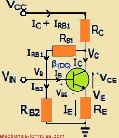
Using Dual Feedback BJT Biasing
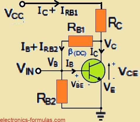
VC = VCC - RD(IC + IB1)
VE = 0V
VB = VBE
IRB2 = VB / RB2
IRB1 = IB + IRB2 = (VC - VB) / RB1
IC = β(DC) * IB
IE = (IC + IB) ≅ IC
When we think about adding an extra resistor to the base bias network from our previous setup, we actually find that it really boosts stability even further when it comes to variations in gain Beta (β) of the BJT. This happens because we are increasing the current that flows through those base biasing resistors which looks pretty neat.
Now typically, the current that flows through RB1 is set to be around 10% of the collector current IC. But we have to keep in mind that this current also needs to be higher than the base current that is necessary for the minimum value of Beta (β). It is all about making sure we have enough current to keep things running smoothly.
One of the cool things about this self-biasing configuration we are using is that those two resistors are doing double duty. They not only provide automatic biasing but also give us Rƒ feedback at the same time. It is like getting two benefits in one setup.
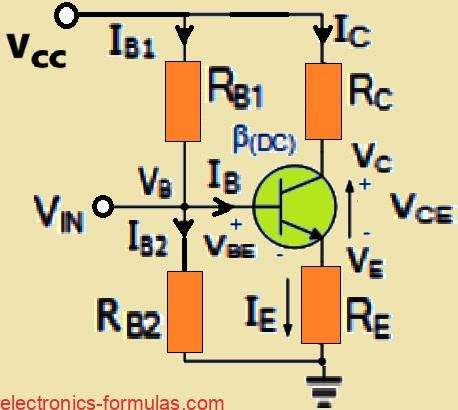
Using BJT Emitter Feedback Circuit
VC = VCC - RD(IC + IB1)
VE = IE * RE = VB - VBE
VCE = VC - VE
VB = VBE + VE
IRB2 = VB / RB2
IRB1 = IB + IRB2 = (VC - VB) / RB1
IC = β(DC) * IB
IE = (IC + IB) ≅ IC
In this setup, we leverage both emitter and base-collector feedback mechanisms to give that extra stability to the collector current. Why does this happen you may ask? Well, it is all about how resistors RB1 and RE along with the base-emitter junction of our transistor, are effectively linked in series with the supply voltage VCC.
The Trade-off: Output Gain
However we should keep in mind that there is a bit of a downside to this emitter feedback configuration. It tends to reduce the output gain and that is primarily due to the way the base resistor is connected.
The collector voltage plays a pivotal role here, it determines the current flowing through our feedback resistor RB1 which leads to what we call “degenerative feedback.”
The Emitter Current Dynamics
Now let us talk about the current flowing from the emitter IE. This current is actually a combination of IC (the collector current) and IB (the base current). As IE flows through RE, it causes a voltage drop that appears in such a way that it reverse biases the base-emitter junction.
So if the emitter current increases—let us say because there is an uptick in collector current—then the voltage drop across I*RE also rises.
Since this voltage has a polarity that reverse biases our base-emitter junction, what happens next is quite fascinating: IB automatically decreases! This means that even though the emitter current is increasing, it will not rise as much as it would have if there had not been any self-biasing resistor in play then.
Setting Resistor Values for Optimal Performance
In general practice we usually set our resistor values so that the voltage drop across our emitter resistor RE is about 10% of VCC. Similarly we aim for the current flowing through resistor RB1 to be around 10% of our collector current IC.
Using Voltage Divider BJT Biasing
VC = VCC - RC * IC = (VE + VCE)
VE = IE * RE = VB - VBE
VCE = VC - VE = VCC - (IC * RC + IE * RE)
VB = VBE + VE = VRB2 = (RB2 / (RB1 + RB2)) * VCC
IB2 = VB / RB2
IB1 = IB + IB2 = (VCC - VB) / RB1
RB = (RB1 * RB2) / (RB1 + RB2)
IB = (VB - VBE) / (RB + (1 + β) * RE)
IC = β(DC) * IB
IE = IC + IB = VE / RE
So basically when we are talking about setting up a common emitter transistor, we often use what is called a voltage divider network to keep things nice and stable.
The reason it is called “voltage divider biasing” is pretty straightforward: we have two resistors RB1 and RB2 which act like a voltage or potential divider. They are connected across the power supply and their middle connection point is hooked up to the transistor’s base terminal, just like you see in the diagrams.
This voltage divider biasing setup? It is like the go-to method for biasing transistors. The transistor’s emitter diode gets forward biased due to the voltage developed across that resistor RB2.
And here is a cool thing, with this voltage divider network biasing, the transistor circuit does not really care if the Beta changes because the biasing voltages at the transistor’s base, emitter, and collector terminals are not affected by external circuit values.
Now if we want to figure out the voltage across RB2 which is also the voltage applied to the base terminal, then we just use the good old voltage divider formula for resistors in series.
Usually the voltage drop across RB2 is much smaller than the voltage drop across RB1. So it is pretty obvious that the transistor’s base voltage VB with respect to ground, is the same as the voltage across RB2.
To make sure the voltage divider is doing its job properly, we usually set the current flowing through RB2 to be ten times the base current IB that we need. This way it is high enough that it does not mess up with the voltage divider current or any Beta changes.
The whole point of Transistor Biasing is to get a stable quiescent operating point or Q-point, so the bipolar transistor works efficiently and gives us a nice, undistorted output signal. Getting the DC biasing right also sets up the initial AC operating region and we usually use either a two or four-resistor bias network for this.
In bipolar transistor circuits, we represent the Q-point as (VCE, IC) for NPN transistors or (VEC, IC) for PNP transistors. To see how stable the base bias network is and therefore the Q-point, we usually look at how the collector current changes with both Beta (β) and temperature.
So we have taken a quick look at five different ways to “bias a transistor” using resistive networks. But hey, we can also bias a transistor using silicon diodes, zener diodes, or active networks, all connected to the transistor’s base terminal. And if we want then we could even bias the transistor correctly from a dual voltage power supply!
References:
Leave a Reply