
In my practical works, when connecting digital logic gates to external circuits or devices, I personally ensure that their inputs and outputs are properly set to provide the correct switching conditions. This is where Pull-up Resistors come into play, because they help make sure that the inputs or outputs are functioning as per the expectations.
Modern forms of digital logic gates, integrated circuits (ICs), and microcontrollers come with multiple inputs also referred to as the “pins,” and with one or more outputs. For the digital circuit to work correctly, we have to make sure that we configure these inputs and outputs properly to either a HIGH logic or a LOW logic states.
We by now pretty well understand that logic gates are the fundamental elements of any digital circuit. And, by combining the three basic gates, which are the AND, OR, and NOT, it becomes possible for us to build complex combinational digital logic circuits. Since these circuits are digital, they operate with only two logic states, logic “0” and logic “1.”
These logic states are represented by different voltage levels. Any voltage that may be below a certain threshold is considered to be a logic “0,” and any voltage which may be above another threshold is considered to be a logic “1.” For instance, suppose if the voltage levels are 0V and +5V, then the 0V would be interpreted as logic “0,” and the +5V would be logic “1.”
If in a situation the inputs to a digital logic gate or circuit fall outside the range required for proper detection of logic “0” or logic “1,” then your circuit might start malfunctioning. This can happen if the HIGH value is not sufficiently high enough or the LOW value is not sufficiently low enough, causing the gate or circuit to misinterpret the input voltage values.

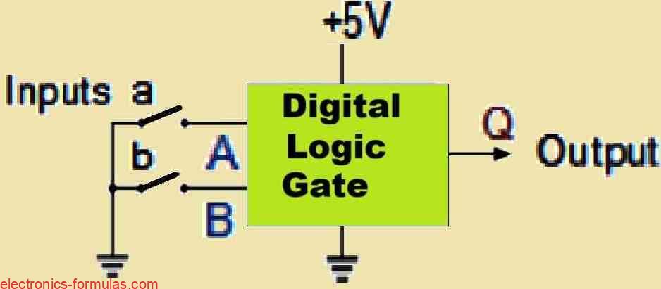
Let us consider an example as shown in the figure above, by involving a digital circuit. On the left side, we can see there are two switches, labeled “a” and “b,” which serve as inputs to a generic logic gate. When we close switch “a” (ON), input “A” is connected to ground (0V) or logic level “0” (LOW). In the same manner, by closing switch “b” (ON) connects input “B” to ground, making it logic level “0” (LOW).
This setup is what we actually need.
But, when we open switch “a” (OFF), the voltage at input “A” might become uncertain. We might expect it to be +5V (HIGH) because the switch is open, so input “A” is not connected to ground. But that is not always the case. With the input now disconnected from a clear HIGH or LOW state, it might “float” between 0V and +5V (Vcc), which can potentially settle down at any voltage level, and this could be interpreted as either HIGH or LOW by the digital gate.
The above explained floating condition might cause the input “A” to inadvertently remain at a logic “0” (LOW) when we actually need a logic “1” (HIGH), which might in turn result in the logic gate incorrectly switching the output at “Q.” Additionally, we may see that this unstable and weak input signal might easily change with even minor interferences or noises from adjacent inputs, or even initiate oscillations, making the gate practically, very unusable. The exact same issue also applies to the input “B.”
So, to prevent such problems and avoid unintentional switching in our digital circuits, we need to ensure that any unconnected inputs, known as “floating inputs,” are tied to a well defined logic level, either HIGH or LOW, as required by the circuit. We can easily and effectively achieve this simply by using Pull-up Resistors or Pull-down Resistors, which ensure that the input pin has a consistent default state, whether the switch is open, closed, or disconnected.
While building digital electronic circuits, we mostly might have extra gates or latches within an integrated circuit (IC) package that go unused, or a multi-input gate may have some inputs that are not connected. Always make sure to tie these unused logic inputs to a fixed voltage using a high-value resistor connected to Vcc (pull-up) or a low-value resistor connected to 0V (GND) (pull-down). It is very crucial that we do not leave these inputs floating at all.
Understanding Pull-up Resistors
To prevent the inputs of digital logic gates and circuits from floating or self-biasing, we typically connect any unused pins either directly to ground (0V) to ensure that a stable low “0” input for OR and NOR gates, or we connect it to Vcc (+5V) to maintain a steady high “1” input for AND and NAND gates. Let us now refer to the two switched inputs diagram that we discussed above.

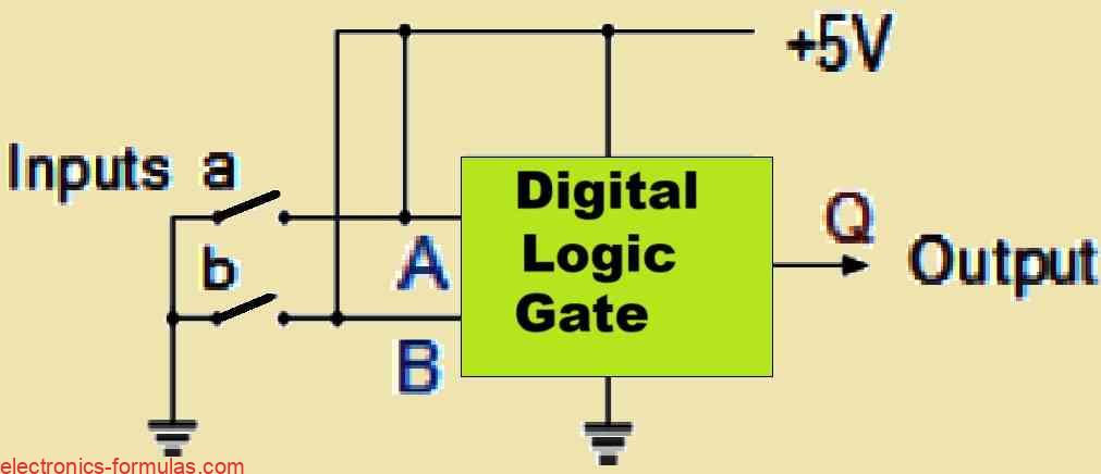
In order to avoid having inputs A and B float when switches “a” and “b” are open (OFF), we connect these inputs to the +5V supply.
At the first observation you might think that this approach is effective because, with switch “a” open (OFF), the input is linked to Vcc (+5V), and when the switch is closed (ON), the input is grounded as before, which thus keeps inputs A and B at a consistent default state regardless of the switch’s position.
However you will find that this setup has a critical flaw, because when we close either of a switch (ON), it creates a direct short circuit between +5V and ground, which can lead to a very high current that could blow a fuse or damage the circuit. So to address this problem, we can simply use a pull-up resistor connected between the input pin and the +5V supply, as illustrated below:
How to Connect and Implement a Pull-up Resistor in a Circuit

With the help of the two pull-up resistors, one for each input, we ensure that when switch “A” or “B” is turned off, the input is effectively connected to the +5V supply via the pull-up resistor. This configuration might result in a minor voltage drop across the pull-up resistor when the logic gate receives a small input current. Therefore practically the whole +5V supply voltage reaches the input pin, resulting in a HIGH, logic “1” condition.
Now as soon as switches “A” or “B” are closed (ON), the input of the gate gets connected directly to ground (LOW), resulting in a logic “0” at the input. In this condition we are able to effectively avoid shorting of the supply rail because of the presence of the high value pull-up resistor which allows barely any current to travel through the closed switch to ground.
The above technique of using a pull-up resistor guarantees that the input always has a consistent, specified logic state, either HIGH or LOW, depending on the position of the switch. By preventing the input from floating or self-biasing, this configuration ensures a proper output function at the gate’s “Q” terminal and produces the intended switching action flawlessly.
You may find it a common practice to connect Vcc to an input or output with a pull-up resistor, but calculating the correct values of the resistance to guarantee proper operation might look difficult, right? In the next paragraph, we will discuss how we can calculate the correct pull-up resistor values.
How to Calculate a Pull-up Resistor
When working with digital logic gates, circuits, and microcontrollers, we must consider both their operating voltage and the current sourcing and sinking capabilities of each input pin. Digital logic circuits therefore, depend on two binary states, which are a high voltage (VH) for logic “1” and a low voltage (VL) for logic “0.” Moreover each of these states is represented by a range of voltages, which defines the upper and lower limits within which these binary states work as valid supply levels. Therefore it is important for us to understand these voltage ranges for ensuring a proper circuit functionality.

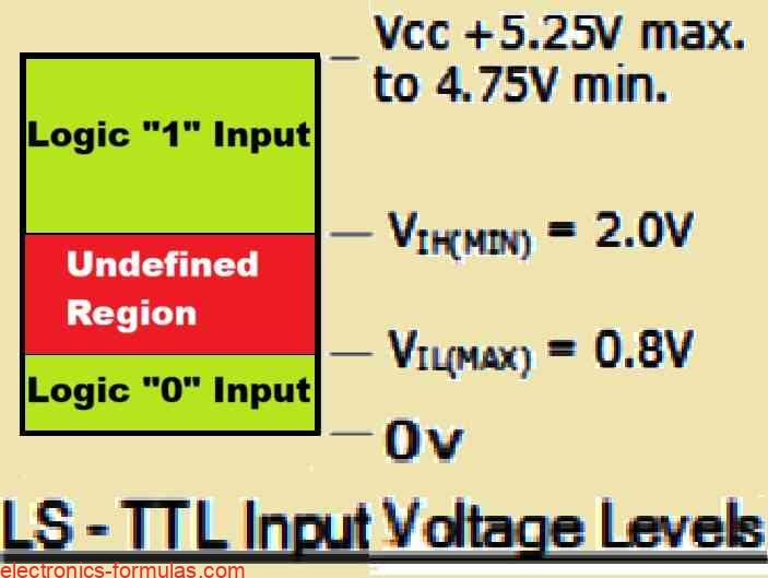
For instance, referring to the diagram above, in the TTL 74LSxxx series of digital logic gates we find that the voltage ranges defining a logic level “1” and a logic level “0” are specified. To be precise VIH(min) = 2.0V represents the minimum input voltage guaranteed to be recognized as a logic “1” (high) input, whereas VIL(max) = 0.8V denotes the maximum input voltage guaranteed to be recognized as a logic “0” (low) input.
In other words input signals between 0 and 0.8V are regarded as “LOW,” while those between 2.0 and 5.0V are deemed as “HIGH.” Consequently any voltages between 0.8V and 2.0V may not be reliably recognized by the gates as either logic “1” or logic “0.”
Furthermore when we connect logic gates together, current will flow between the output of one gate and the input of another. Thus the amount of current required by a basic TTL logic gate input will vary depending on whether the input is a logic “0” (LOW) or a logic “1” (HIGH). In particular a logic “0” will create a current-sourcing action, whereas a logic “1” will induce a current-sinking action.
When the logic gate input is HIGH, current will flow into the TTL input because it will essentially act as a path connected directly to ground. As a result, this input current, IIH(max), will be positive as it flows “into” the gate and typically measures around 20µA for most TTL 74LSxxx inputs.
Conversely when the input is LOW, current will flow out of the TTL input since it acts as a path connected directly to Vcc. Therefore this input current IIL(max), will be negative as it will flow “out of” the gate and generally measures around -400µA (or -0.4mA) for most TTL 74LSxxx inputs.
But, it is important for us to note that, the values for HIGH and LOW voltages and currents can vary between different TTL logic families and are significantly lower for CMOS logic families. Additionally the input voltage and current requirements for microcontrollers such as PICs, Arduinos, or Raspberry Pis also differ, so we must always check their datasheets for specific details before delving into a digital circuit project.
So, with reference to the above considerations, it is possible for us to calculate the values of an optimal pull-up resistor value for any TTL 74LS series logic gate in the following manner:
RMAX = (VCC – VIH(MIN))/IIH
= (5 – 2)/(20 * 10-6)
= 150 kΩ
According to Ohm’s Law, we calculated the maximum pull-up resistor resistance that would create a drop of 3 volts for a TTL 74LS series logic gate to be 150 kΩ. Although this should work as intended, the calculated resistor value will not inherently give you any headroom for error. Specifically, the voltage across the resistor has to be at the calculated maximum value while the input current will be at its minimum.
It would be ideal for the logic “1” to be situated as closely to Vcc as possible, thereby assuring that the logic IC gate is seeing a HIGH (logic-1) logic voltage through the pull-up resistor. If you wanted to account for more tolerance in case the tolerance of the resistor, or the supply voltage, is off, and you wanted to still have reasonable current through the logic IC, you would select a lesser resistor value, However, we just have to be careful not to go too far with the resistor, because if the resistor is too small, the amount of current going through the logic IC will be larger and thus the power dissipated by the pull-up resistor will be larger.
Assuming the applied resistor has a voltage drop of only 1 volt, that would yield 4 volt of output voltage into the TTL gate, therefore we can calculate the pull-up resistor of 50kΩ. Reducing the resistor value would reduce the voltage drop, while increasing the current.
Clearly, there is a maximum resistor value that can work well in biasing a single TTL gate, and again, that pull-up resistor value does not need to be critical. Generally, the pull-up resistor value is typically in the range of 10kΩ to 100kΩ.
This may indicate a maximum pull-up resistor value needed for one TTL gate, however the same pull-up resistor can be used to bias multiple inputs to the logic value “1”.
For example, assuming we have a digital circuit with a total of ten unused logic gate inputs and each standard TTL 74LS gate has an input current (IIH(max)) of 20μA. This means that 10 TTL gates will draw a total of 200μA of current, this represents a fan-in of 10.
Calculating Pull-up Resistor Value for Multiple Gates
So now we can calculate the maximum value of the pull-up resistor necessary for supplying ten unconnected inputs in the following manner:
RMAX = (VCC – VIH(MIN))/(10 * IIH)
= (5 – 2)/(10 * 20 * 10-6)
= 15 kΩ
We see that there is a fan-in of 10 in this case. However if we connect ‘n’ TTL inputs together, the current through the resistor will equal ‘n’ times the maximum input high current (IIH(max)) mentioned previously.
We said before that the 15kΩ value might be the exact calculated value, but here there is no tolerance. If we would like to have a more agreeable voltage drop, let us make it easier and say we want to reduce it to one volt. In that case, we can recalculate the resistance, and we will come up with only 5kΩ
Solving a Pull-up Resistor Problem #1
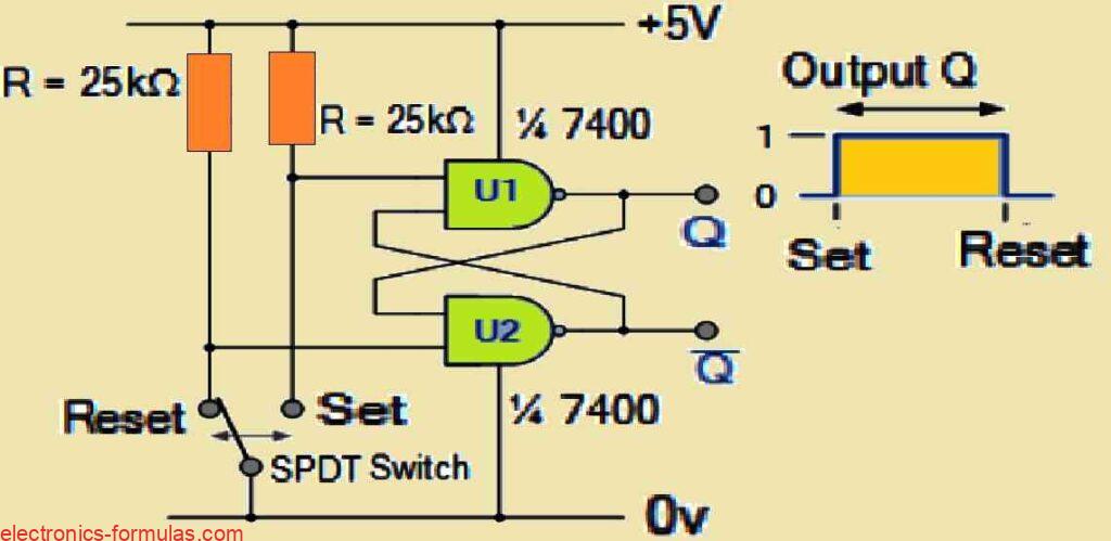
Let us design a basic Set-Reset flip-flop using two TTL 74LS00 NAND gates and a single pole double throw switch (SPDT).
Here we need to: Calculate what is the maximum value we can use for the pull-up resistor to guarantee a 4.5v logic HIGH on the input with the switch open. Calculate the current through the pull-up resistor when the switch is closed, take contact resistance to be zero. Make a circuit diagram to show your solution.
1) First we calculate the RMAX pull-up resistor value:
RMAX = (VCC – VIH)/IIH
= (5 – 4.5)/(20 *10-6)
= 25 kΩ
2) Then we calculate the current through the resistor:
IR = VCC/R
= 5V/25kΩ
= 200 μA or 0.2 mA
So, the Circuit Diagram for the above Calculated Set-Reset Bistable Circuit will be:

Understanding Pull-down Resistors
When we employ a pull-down resistor, its action is very much like that of a pull-up resistor, but instead of being connected to a positive voltage, we connect it to ground, which sets the logic level to “0” (LOW). In this way, the input can toggle to HIGH whenever we actuate the mechanical switch.
Pull-down resistors are especially useful in digital circuits such as latches, counters, flip flop circuits. With pull-down resistors, we can ensure that we get a reliable positive one-shot trigger whenever a switch is operated for a short period of time, which can result in the change of the logic state.
Even though a pull-down resistor appears to work just like a pull-up resistor, we must be a little more cautious with its resistive value for TTL logic gates when compared to CMOS logic gates. This is because TTL logic gates draw much more current from their input in the LOW state.
For example, in the case of TTL 74LSxxx series logic gates, this logic “0” (LOW) is pulled LOW, with a maximum voltage of 0.8 volts (VIL(MAX) = 0.8V). When the gate is LOW, it will source a current of 400μA (IIL), so it can be said that each TTL logic gate therefore pulls 400μA source current to the input.
Using the all the above information we can now calculate the maximum value for a pull-down resistor for a single TTL logic gate, as explained below:
Calculating Pull-down Resistor Value for a Single Logic Gate
RMAX = (VIL(MAX) – 0)/IIL= (0.8 – 0)/(400 * 10-6)= 2 kΩ
From the above calculations we have determined that the maximum value for the pull-down resistor is 2kΩ. Just like the pull-up resistor calculations, this 2kΩ value is chosen because it ensures the voltage drop is maximized, leaving no margin for error.
If the resistance were too high, the voltage drop across the pull-down resistor might push the gate input voltage outside the acceptable logic LOW voltage range. So to guarantee proper switching, it is best to maintain the input voltage at 0.5 volts or lower.
How to Implement Pull-Down Resistors


Taking into account a negligible voltage drop of 0.4 volts across the pull down resistor, we can see that a resistor value of 1kΩ would just suffice. It also means that if we were to reduce the resistance further it would lead to a more significant voltage drop effectively grounding the input.
Although you will find that the datasheet specifies a minimum LOW current value of 400μA or 0.4mA (IIL) but based on my observations I can say that the actual current could exceed this threshold.
Now, suppose if we connect multiple inputs together it would increase the current passing through the resistor.
For example with a fan-in configuration of 10 we would require a pull down resistance of 100Ω to handle the resulting 4.0mA current.
Now, suppose if we directly ground the input, that may seem to be quite adequate for establishing a logic LOW state, but employing a pull down resistor provides several more benefits. The pull-down resistor helps to limit the current flowing out of the input thus reducing power consumption while also maintaining the logic LOW state.
Logic ICs that have Open-collector Outputs
So far we’ve explored how we can modify the voltage level of a logic gate through pull up or pull down resistors. However it’s worth noting that pull up resistors on the output of a gate can also serve the purpose of linking different gate technologies like connecting TTL to CMOS or driving transmission lines in situations that require higher currents and voltages.
To address this issue certain logic gates are designed with the collector of their internal output circuit not connected or floating. This means that the job of the logic gate output is only to create a logic LOW by grounding through the collector, while the task of pulling it to logic HIGH is separately handled by external pull up resistor connected across the collector and the positive line. A notable example of this design can be found in the TTL 74LS01 Quad input NAND gate featuring open collector outputs unlike the standard TTL 74LS00 Quad input NAND gate, which does not have this capability.
In buffer inverter and driver ICs (such as TTL 74LS06 and 74LS07) open collector (OC) or open drain (OD) outputs are commonly used. These outputs can handle higher current or voltage levels compared to standard logic gates. For example they can be employed to drive loads such as a motor, a small relay or an LED indicator. In both the cases the pull up resistor functions on the principle same as for the inputs.
Open Collector Outputs

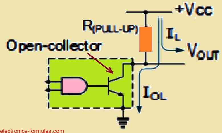
In digital circuits such as logic gates and microcontrollers the use of open collector outputs means they cannot send signals to a HIGH state. This is because they lack a direct connection to the supply voltage (Vcc). When the output is set to LOW it gets grounded while setting it to HIGH leaves it floating. To make sure everything works smoothly an external pull-up resistor (Rp) must be added. This resistor connects the open collector pin of the gate output transistor to the Vcc supply.
Functioning of Pull Up Resistors
When a pull up resistor is used, the output operates similarly to a regular logic gate. If the output transistor is OFF (open) the output state is HIGH and when it is ON (closed) the output state becomes LOW, effectively bringing the output down to a LOW level. The resistance value of the pull up resistor can be evaluated depending on the load it supports and the voltage drop across the resistor, when the transistor is not conducting.
Current Sinking and Sourcing Needs
In situations where the output is LOW, it is necessary for the transistor to absorb the load current passing through the pull up resistor. On the other hand, when the output is HIGH the current flowing through the pull up resistor should be adequate to support any external connected devices or components
Voltage States in Digital Logic
In digital logic, the functioning of a gate relies on two binary states represented by different voltage levels. A high voltage (VH) signifies logic “1” while a low voltage (VL) denotes logic “0”. Each state has its own voltage range with VOH(min) indicating the minimum output voltage recognized as logic “1” (HIGH), set at 2.7 volts for TTL logic. On the hand, VOL(max) represents the maximum output voltage recognized as logic “0” (LOW), measured at 0.5 volts for TTL IC 74LSxxx. Consequently, output voltages ranging from 0 to 0.5V are classified as “LOW” while those falling between 2.7 and 5.0V are deemed as “HIGH”.
Therefore when you are using a gate which is built with open-collector logic gates, then the pull-up resistors value to be connected across its output and positive line could be calculated using the following formula:
Calculating the Value of Open-collector Pull-up Resistors
RMIN = (VCC – VOL(MAX))/IOL
= (5 – 0.5)/(8 * 10-3)
= 562 Ω
When using a 7401 open collector NAND gate, its specifications include a Vcc of 5V, an output low voltage (VOL) of 0.5V and a maximum output low current (IOL(max)) of 8mA. Choosing a pull up resistor (Rp) is essential since the current through this resistor should not exceed the IOL(max) limit.
Open collector logic gates such as the 7401 are particularly advantageous for controlling loads that require higher voltage and current, like LED indicators. For instance the TTL 74LS06 Hex Inverter Buffer/Driver has a maximum output low current (IOL(max)) rating of 40mA significantly surpassing the 8mA limit of the 7401. Moreover the maximum output high voltage (VOH(max)) rating for the 74LS06 is 30 volts although the integrated circuit itself operates strictly with a 5V power supply. This capability allows the 74LS06 to drive loads needing up to 40mA of current making it more versatile for applications, with higher power requirements.
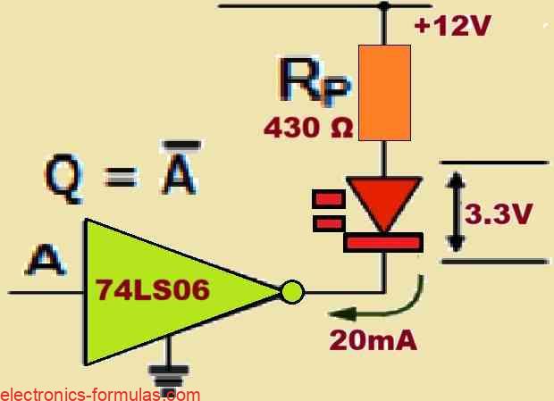
Solving a Pull-up Resistor Problem #2
We want to calculate the current-limiting resistor needed to drive a red LED indicator using a 74LS06 Hex Inverter Driver from a 12V supply, follow these steps:
Get The LED Specifications:
- Forward current (IF) required by the LED: 20 mA (0.020 A)
- Forward voltage drop (VF) across the LED: 3.3 V
Identify the Output Voltage VOL of the Inverter:
- The output low voltage (VOL) of the 74LS06 when fully ON is 0.1V.
Calculate the Voltage across the Resistor:
The total voltage from the supply is 12 V. The voltage drop across the LED is 3.3 V, and the output voltage of the inverter when ON is 0.1 V.
Therefore, the voltage across the current-limiting resistor (VR) can be calculated as:
VR = Vcc – VF – VOL
Substituting the values:
VR = 12V – 3.3V – 0.1V = 8.6 V
Calculate the Value of the Resistor (R):
Using Ohm’s Law (V = IR), we can rearrange it to find the resistance:
Rp = VR / IF
Substituting the values:
Rp =8.6V / 0.020 A = 430 Ω
Circuit Diagram

Open collector drivers can be utilized to operate small electromechanical relays, lamps or DC motors as these devices generally require voltages ranging from 5V to 12V or even higher with a current of approximately 10 to 20 mA for optimal functioning. When we link two or more open collector outputs of TTL gates together and connect them through a single external pull up resistor the outputs essentially mimic the behavior of an AND gate. This configuration, known as wired AND logic enables us to merge multiple signals such that the output is triggered only when all connected outputs are in a low state.
Conclusions
In this tutorial we explored the concept of passive pull up and pull down resistors. It was highlighted that when the inputs of logic gates are left open circuited they can self bias or float to any logic level they prefer. This can lead to switching errors that are often caused by unconnected and floating input pins.
We can use Pull-up resistors to connect input pins of AND and NAND gates to the supply voltage Vcc to ensure that the input remains in a HIGH state. On the other hand pull-down resistors are employed for input pins of OR and NOR gates, connecting them to ground (0V) to keep the input at a LOW level. Although the resistance value for a pull-up resistor is not typically critical it should be sufficient to keep the input pin voltage above the threshold voltage VIH. Commonly 10kΩ pull-up resistors are used, but for most applications you can use any value between 1k to 100k ohms.
Pull-down resistors play a role in ensuring proper functioning of logic gates especially in scenarios with low input voltage levels (VIL(max)) and higher IIL currents. While 100Ω pull down resistors are commonly used, their resistance values can range from 50 to 1k ohms.
In the case of digital logic gates that have open collector outputs for TTL logic or open drain outputs for CMOS logic, an external pull-up resistor will be needed. This resistor should be connected between the output pin of the gate and the DC power supply to ensure the logic gate operates, as intended.
Utilizing open collector or open drain gates offers us with some good benefits, which includes the ability to handle voltages and currents and the functionality of wired ANDing. Certain open collector gates like the 74LS06 can support loads, because their outputs can be linked to power sources of up to 30 volts through an external pull-up resistor.
References: what does pull-up resistor and pull-down resistor mean? How do I implement them in my circuit?