
Throughout my electronics career I have found the Sallen-Key filter to be an excellent tool in my circuit design toolset. It is an active filter… which means it shapes the signal using devices such as op amps. What makes it so attractive is actually its simplicity and adaptability.
How Does It Work?
A Sallen-Key filter consists of an op-amp, two resistors, and two capacitors. This combination results in a voltage-controlled voltage source (VCVS) circuit. The beauty of this design is its high input impedance, low output impedance, and great stability.
Another advantage of Sallen-Key filters is that We can combine many of these together to construct even more complicated filter designs.
Understanding the Basics of RC Networks
Before we investigate deeper into Sallen-Key filters, it is important for us to understand how the fundamental resistor-capacitor (RC) networks may respond at various frequencies. This information is critical for understanding how the Sallen-Key filter would work.
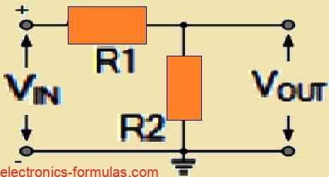
The Resistive Voltage Divider – a simple way to reduce voltage.
Whenever we need to convert a larger voltage into a lower voltage, we mostly utilize a voltage divider circuit. It is a simple circuit consisting of two (or more) resistors linked in series across a power source. This basic system divides the input voltage into smaller outputs.

How Does It Work?
Consider a water pipe with two sections. The broader portion allows greater amounts of water to flow, but the narrower portion inhibits it. In a similar manner resistors in a voltage divider regulate voltage distribution.
We know that according to Ohm’s Law, the voltage across a resistor is proportional to both the current flowing through it and its resistance. So if we use two equal resistors, the voltage would be divided equally between them.
The output voltage is measured across one of the resistors, generally the one closest to ground, which is R2 in the figure above. The ratio of resistor values influences the output voltage with respect to the input voltage. This relationship may be stated using the following formula:
Av = Vout/Vin = R2/(R1 + R2).
∴ Vout = Vin[R2/(R1 + R2)]
Voltage Dividers and AC Supply
A cool thing about voltage dividers is that they work the same way with both AC and DC voltages. Resistors generally do not care about frequencies, meaning the voltage division in resistive divider circuits happens regardless of the input voltage type.
If we change the input voltage to an AC source and alter its frequency, what will happen to the output voltage VOUT of the RC divider?
Remarkably nothing changes at all, because resistors are normally unaffected by the variations in frequency (with the exception of wire-wound resistors), meaning their frequency response is flat. This means that AC voltages, expressed as I2rms * R, build up across the resistors in the exact same way as steady-state DC voltages.
Changing Resistor R1 to Capacitor C to Create RC Potential Divider.

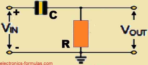
When We replace the resistor R1 in our circuit to a capacitor C, it has a major effect on the transfer function. Here is how.
Capacitor Behavior at DC Voltage
Now we already know that, when a capacitor is completely charged and attached to a DC voltage source, it behaves like an open circuit. This means that when we supply a steady-state DC voltage to VIN, the capacitor will eventually charge to its maximum voltage.
Charging Time and Current Flow
The time constant T, which is the product of resistance R and capacitance C, determines how long it takes for the capacitor to get fully charged. More specifically, the capacitor is considered fully charged at 5 time constants or 5T = 5RC. During the charging process, the capacitor takes current from the DC source.
As soon as the capacitor has been fully charged, no current flows through it, because, under steady-state circumstances, the capacitor behaves like an open circuit.
This consequently means that no current flows through the resistor R connected in series with the capacitor, hence there is no voltage drop across R. As a result, no output voltage will be generated in the circuit where the resistor R is intended to generate a voltage drop.
Capacitors will block DC voltages.
From the above discussion we understand that capacitors block steady-state DC voltages once fully charged. Replacing R1 with a capacitor C in the transfer function would imply that the capacitor effectively stops any DC current from flowing through the resistor R, resulting in no output voltage in the steady state situation.
Analyzing Capacitor Behavior in Frequency
To understand the above behavior we need to analyze the circuit in the frequency domain. This means that we now focus on how the circuit responds to signals which tends to change over time.
Capacitive Reactance
One important concept here is the capacitive reactance (XC), which is actually the capacitor’s opposition to the flow of alternating current or AC and this is measured in ohms. But unlike resistance capacitive reactance will vary in accordance with frequency.
Frequency Dependence of Capacitive Reactance
When we have lower frequencies (f ≅ 0), the capacitor will behave almost like an open circuit, which can produce significant limitations to the current flow. So, that also means that now as the frequency increases, capacitive reactance decreases, which now allows higher amounts of currents to pass through.
The capacitor acts as a short circuit and passes the signals straight to the output as VOUT = VIN when the frequencies are extremely high (ƒ ≅ ∞). But despite this, the capacitor exhibits the impedance indicated by XC which lies somewhere in the middle of these two frequency extremities. As a result, the voltage divider transfer function we obtained above, now becomes:
Av = Vout/Vin = R/(R + XC)
This means that as the frequency changes it causes changes in XC, which in turn results in the alterations in the level of the output voltage.
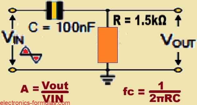
RC Filter Circuit
Now, let us take the example of the following the circuit design:


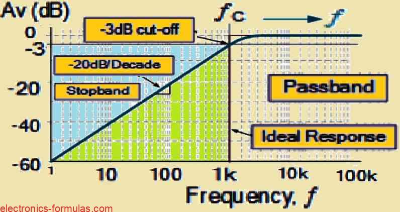
In the above graph we can clearly visualize the frequency response of the adjoining1st order RC circuit. We see that in response to lower frequencies the voltage gain tends to be very very low, because the reactance of the capacitor tries to block the input signal frequencies.
But as the frequency increases to higher levels the voltage gain becomes high (unity) because now the reactance of the capacitor causes the capacitor to generate an substantial short-circuit to these high frequencies, which means now VOUT = VIN
But despite this, we come across a frequency point wherein the reactance of the capacitor becomes equal to the value of the resistor, meaning now: XC = R. This situation is termed as the “critical frequency” point, or simply the cut-off frequency, or the corner frequency fC.
From the above information we see that the cut-off frequency is generated when XC = R, so the standard equation that we can use to calculate this critical frequency point is as follows:
fc = 1/2πRC
The cut-off frequency, written as fc is an important parameter in a circuit that controls how it filters signals. In the context of a high-pass filter, fc is the frequency threshold at which the circuit switches from attenuating (lowering the amplitude of) frequencies below fc to allowing frequencies above fc to pass through with minimum attenuation.
In simple terms, a high-pass filter rejects signals with frequencies less than fc but will allow signals with frequencies that are higher than fc to pass.
The cut-off frequency is the point where the ratio of the input-to-output signal gets the value of 0.707 and which translates to –3dB in terms of decibels. Sometime we also call this as the filter’s 3dB down point.
Because the capacitive reactance (XC) is inversely proportional to the applied frequency, we can revise the voltage divider equation above to obtain the transfer function of this straightforward RC high pass filter circuit, as shown in the example below:
Av = Vout/Vin = R/(R + XC)
Since XC = 1/2πfC
∴ Vout / R/[R + (1/2πfC)]
= 2πfRC/(1 + 2πfRC)
Disadvantage of RC Filter
Obviously, you will find that the main disadvantages of an RC filter is that the output amplitude can never be higher than the input amplitude which means that the gain of this filter can never be higher than unity.
Another thing is that the filter’s output when applied with external loading through more number of RC stages or circuits this negatively impacts the characteristics of the filter.
Mitigating the Problem with an Op-Amp
But you can find one method to counter this problem, that is by converting the passive RC filter into an “Active RC Filter” which can be done by introducing an operational amplifier to the fundamental RC filter circuit design.
Now when we add this operational amplifier to the basic RC filter circuit it enables the circuit to produce intended amount of voltage gain across its output, which transforms this RC filter from an attenuator to an amplifier.
Moreover, because the op-amp exhibits a high input impedance and low output impedance it simply eliminates any form of external loading on the filter, which means now it becomes easy for us to achieve a wide adjustable range frequency from this circuit ensuring that the desired frequency response is never impacted.
Circuit Diagram of an RC Active High Pass Filter
Please refer to the following simple active RC high-pass filter as shown below:

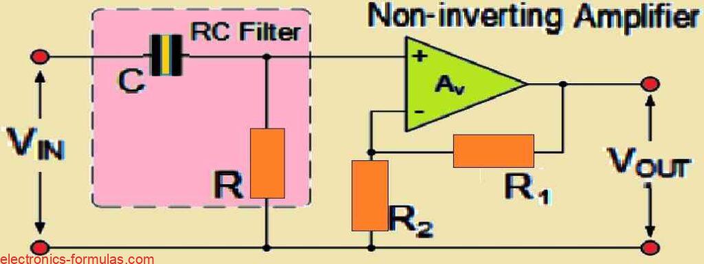
In this diagram the RC stage of the design behaves in the same manner as we discussed earlier above. Meaning, the RC stage will allow all the high frequency signal content but block the low frequency content of the signal.
The cut-off frequency of this RC stage is determined by the values of the existing resistor and the capacitor (RC). The op-amp as can be seen has been setup like a non-inverting amplifier circuit, and the gain of this amplifier is decided through the values of the resistors R1 and R2.
Formula for Calculating Cut-off Frequency
With the above situation, the closed loop voltage gain AV in the passband frequency range of the non-inverting operational amplifier can be presented as follows:
AV = 1 + R1/R2
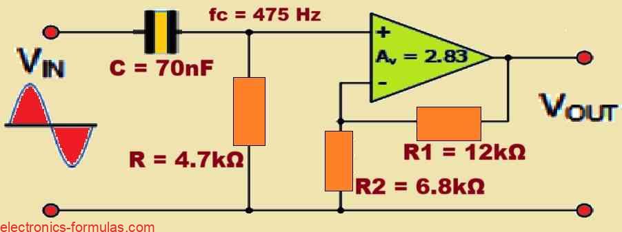
Solving an RC Filter Circuit Problem #1
Consider a simple first order active high-pass filter circuit. In this circuit we want the cut-off frequency to happen at 475 Hz with a passband gain of 9 dB. We want to calculate the appropriate component for implementing the above. For the op-amp we can consider using any common op-amp like the IC 741.
From our earlier discussion we know that the cut-off frequency fC can be calculated by setting up the values of R and C in the RC circuit stage which determines the frequency selection. Let us first arbitrarily select the value for R as 4.7 kΩ (although we can also select any other reasonable value). Next, we can calculate the value of the capacitor C as given below:
fc = 1/2πRC = 475 Hz
Now since R = 4.7 kΩ
∴ C = 1/2 * π * fc * C = 1/2 * π * 475 * 4700 = 71.20 nF
From the above calculations we find that the corresponding value of C to be around 71.20 nF, or 70 nF as the nearest value.
Now, we want the gain of our high-pass filter should be +9dB at the pass band region. This gain corresponds to a voltage gain AV of 2.83. Let’s select a desired random value for our feedback resistor R1 as 12 kΩ, then we can calculate the R1 resistor value as per the following caculations:
9 dB = 20log(A)
∴ A = 2.83
A = VOUT/VIN = 1 + R1/R2 = 2.83
Let’s select the value for R1 to be 12 kΩ
∴ R2 = R1/(A -1) = 12000/(2.83 -1) = 6557 Ω
From the above calculations we get the value of R2 as 6557 Ω or 6.8 kΩ, which appears to be the nearest value.
Finalized High Pass Filter Circuit Diagram
Using the above component values we can now draw our finalized high-pass filter circuit as shown below:

From the above discussion we exactly know that a simple first-order high-pass filter circuit can be designed by setting up a single resistor and a single capacitor (R and C) to generate a cut-off frequency fC point having an output amplitude that is -3dB down from the input amplitude.
Now, if we want to convert the above circuit into a second-order high-pass filter, we just need to add a second RC filter stage with the existing RC filter stage.
Designing a Second-order RC Filter
As shown above, the two RC stages are usually connected in series to construct a simple second-order RC filter. The two RC stage’s input and output impedances must be suitably configured so that they do not interfere with each other’s working, that is, they must function independently for this simple configuration to work as intended.
Passive High Pass Filter Circuit

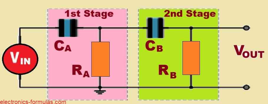
Integrating one RC filter stage to another in cascaded form, regardless of whether they have the same or different RC values, happens to be inefficient. This is because the cut-off frequency shifts further away from the original design value when more stages are added since each new step causes loading of the one stage behind it.
In order to eliminate this issue in the above passive filter design, we should ensure that the input impedance of the second RC stage is at least ten times higher than the output impedance of the first RC stage. In practical terms this means that we need to set the RB value to 10 times R1 and CB to CA/10 at the cut-off frequency.
Now when we increase the component values by a factor of 10 it gives us the advantage of a second-order filter with a steeper roll-off of 40dB/decade compared to the cascaded RC stages. But if we want to design a 4th or 6th-order filter if we just multiply the component values it can be quite time-consuming and complex.
So a simpler method that we can use to create higher-order filters in which individual stages do not interact or load each other, and do not need to be identical, is to employ Sallen-Key filter stages. This simple method allows us to cascade RC filter stages effectively which can make it easier to fine-tune and achieve the required voltage gain.
Understanding Sallen-Key Filter Circuit Main Features
The Sallen-Key configuration is actually one of the most popular choices for designing first-order (1st-order) and second-order (2nd-order) filters, simply because it can be used like a basic foundation for building higher-order filters.
The main features included in a Sallen-Key filter design provides us with the following advantages:
- It is simple and easy to understand.
- It incorporates a single non-inverting amplifier to boost voltage gain.
- It provides us the facility to easily cascade first and second-order filter designs.
- It is flexible and easy to cascade low-pass and high-pass stages together.
- It provides with the option to have different voltage gains for each RC stage.
- It provides us with the facility to easily replicate the RC components and amplifiers.
- The Second-order Sallen-Key stages provide us with a steeper 40dB/decade roll-off compared to cascaded RC stages.
Practical Limitation
The Sallen-key filter is although very versatile but it can have some inherent limitations because of the fact that the relationship between its voltage gain (AV) and magnification factor (Q) is fixed and constant, due to the use of an operational amplifier. If we want to get a Q value greater than 0.5, then we must make sure the voltage gain is greater than 1, but less than 3, because exceeding 3 may lead to instability in the design.
In the most basic Sallen-key filter circuit we make use of equal value capacitors and resistors (although they can differ) and an operational amplifier that is configured as a unity-gain buffer. Notably, now the resistor or RA is no longer grounded, instead it is providing a positive feedback to the amplifier.
Designing a Sallen-key High Pass Filter Circuit

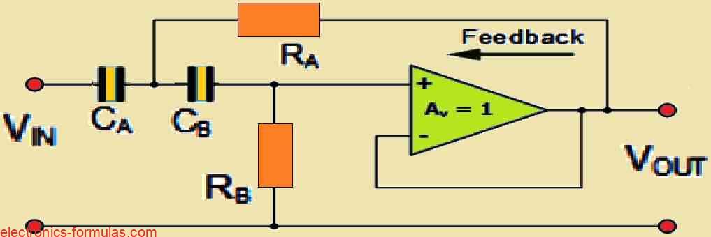
Referring to the above diagram, each of the four passive components—CA, RA, CB, and RB, forms a frequency-selective circuit. When the input is supplied with low frequencies, the capacitors CA and CB behave like open circuits, thus blocking the input signal and generating a zero output.
But when the input signal is supplied with higher frequencies, they start behaving like short circuits which allows the input signal to pass directly to the output.
That said, when the input signal frequency is near to the cutoff frequency, the impedance of CA and CB becomes equivalent to RA and RB. This balance triggers and generates a positive feedback through CB which causes the output signal to amplify and enhance the Q factor of the filter circuit.
Modified Equation for the Sallen-key Cut-off Frequency
Now, as we can see, because there are two sets of RC networks involved in the circuit, our above equation for the cut-off frequency for a Sallen-Key filter gets modified to the following equation:
fc = 1/2π√(RA * RB * CA * CB)
If we make the two series capacitors CA and CB identical to each other (CA = CB = C) and the two resistors RA and RB are also made identical to each other (RA = RB = R), then we are able to make above equation much simpler and resembles the original cut-off frequency equation, as expressed below:
fc = 1/2πRC
Since we have the op-amp circuit rigged as a unity gain buffer circuit, meaning A = 1, the cut-off frequency fC and Q now become totally independent of each other enabling the filter design to become a lot simpler. As a result, the magnification factor Q now can be calculated in the following manner:
Q = 1/(3 – A)
= 1/2
= 0.5
So, as we can see, when the filter circuit is configured as a unity-gain buffer, its voltage gain (AV) becomes equal to 0.5, or -6dB (over damped) when the frequency is at around the cut-off frequency point. Here, this becomes obvious because this is a second-order filter response where 0.7071 * 0.7071 = 0.5. That is -3dB * -3dB = -6dB.
But since Q defines the filter’s response characteristics, choosing the right operational amplifier feedback resistors (R1 and R2) enables us to choose the necessary passband gain A for the selected magnification factor (Q).
Be aware that choosing a value for A that is extremely near to the maximum value of 3 will provide high Q values for a Sallen-key filter architecture. When Q is large, the filter design becomes more susceptible to tolerance fluctuations for the values of feedback resistors R1 and R2.
As an illustration suppose if we adjust the voltage gain of the circuit to 2.9 (A = 2.9), this might cause the value of Q to turn into 10 (1/(3-2.9)), which in turn causes the filter circuit to become extremely sensitive at around the cut-off frequency fC.
Waveform Showing Sallen-key Filter Response Curve

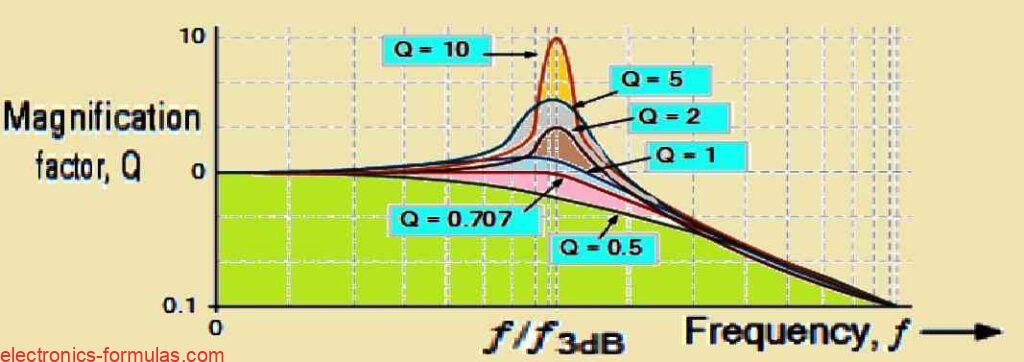
So, in the above Sallen-key Filter Response Curve we can see that when Q of the filter has a lower value the circuit exhibits greater stability, meaning lower the Q, higher the stability. Conversely, higher values of Q could cause the Sallen-key filter to become unstable, but having a very high gains for the design may lead to a negative Q which would in turn result in the generation of oscillations.
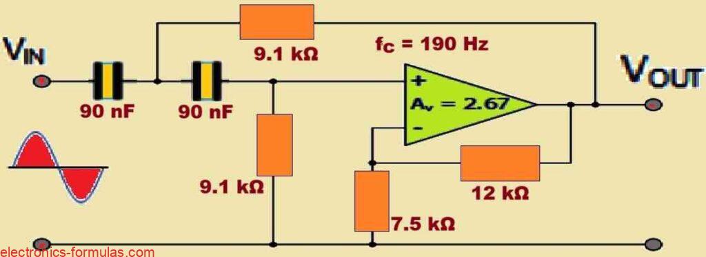
Solving a Sallen-Key Filter Circuit Problem #2
We want to develop a second-order high-pass Sallen and Key Filter circuit having a cut-off frequency fc= 190 Hz, and Q = 2.5.
To make the calculations easier, let us select the two series capacitors CA and CB with identical values (meaning CA = CB = C) and also select the values of the two resistors RA and RB with identical values (meaning RA = RB = R).
fc = 1/2πRC = 190 Hz
Let’s assume the value of C to be 90 nF.
∴ R = 1/(2 * π * fc * C = 1/(2 * π * 190 * 90 * 10-9 ) = 9307 Ω
So we get the value for R as 9307 Ω, or 9.1 kΩ which seems to be the nearest standard value.
With Q = 3, we can calculate the gain with the following equation:
Q = 1/(3 – A)
∴ A = (3Q – 1)/Q
Substituting 3 for the Q, we get:
A = [(3 * 3) – 1]/3 = 2.66
Since now we know the value of A = 2.66, so we know that the ratio of R1/R2 will be 1.66.
Thus, we can calculate the value of R2 using the following formula:
A = VOUT/VIN = 1 + R1/R2 = 2.66
Let’s select the value of R1 to be = 12 kΩ
∴ R2 = R1/(A – 1) = 12000/(2.66 – 1) = 7229 Ω
So the nearest value seems to be 7.5 kΩ, therefore R2 = 7.5 kΩ. With the all the above data gathered, now we can draw the finalized diagram of our Sallen and Key High pass filter as given below:
Finalized Circuit Diagram of the Sallen and Key High Pass Filter using the above data

As we have seen in this lesson, the Sallen-Key circuit design is the most popular filter topology. This topology is also named as voltage-controlled, voltage-source (VCVS) circuit.
The Sallen-Key circuit is the most preferred filter design primarily because the operational amplifier that goes into its design is capable of being set up to function as either a non-inverting amplifier or as a unity gain buffer.
When we use appropriate values of the RC components, then the basic Sallen-key filter design could be utilized to build other filter responses with names like Butterworth, Chebyshev, and Bessel.
We can use the most feasible values for R and C by considering the fact that R and C values are inversely proportional at a given cut-off frequency point. Meaning, when the value of R decreases, C increases, and vice versa.
In order to produce higher-order filters, the Sallen-key which is actually a second-order filter design, may be cascaded with more number of RC stages.
It is not necessary that these additional filter stages should have the same characteristics, such as gain or cut-off frequency. For example, we can construct a Sallen and Key band-pass filter also by combining a low-pass and a high-pass stage.
The conditions that apply to the Sallen-key low-pass filter circuit are the same as those that apply to the Sallen-key high-pass filter circuit that we studied in this article.
For these filters the op-amp’s voltage gain, or AV, controls the overall response of the circuit. The two voltage divider resistors, R1 and R2, specify the voltage gain. It is important to keep in mind that the voltage gain always has to be lower than 3 to prevent oscillation and instability in the filter circuit.
References: Sallen–Key topology