
Before we begin our tutorial on active band pass filter circuits, let’s first look at the passband characteristics of several filter types.
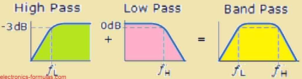
Low-Pass Filters (LPFs): An LPF’s passband begins at 0 Hz (DC) and extends to the set cut-off frequency (fC). This cut-off frequency corresponds to -3 dB with respect to the maximum passband gain. This means the signal strength begins to decrease at fC and continues to decrease at the stipulated rate (usually 20 dB/decade) in the stopband.
High-Pass Filters (HPFs): The passband begins at the -3 dB cut-off frequency (fC) and ideally extends indefinitely. But with active HPFs, the op-amp’s open-loop gain limits the acceptable high-frequency response. As previously stated, the op-amps gain begins to roll off at higher frequencies, eventually limiting the useful passband of the active HPF.
Active Bandpass Filters (BPFs) Block Diagram:

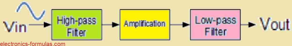
Now lets look at active band-pass filters (BPFs). Unlike LPFs and HPFs, BPFs are intended to be “frequency selective.” To put it simply, they will allow a specified range of frequencies or a “band” of frequencies to pass through, but attenuate all other frequencies that are outside this band.
Band Definition: The desired band of frequencies is specified by two critical cut-off frequencies: fL (lower) and fH (higher). Signals lower than fL and higher than fH are considerably attenuated in the stopband.
Simple Active Band Pass Filter Circuit:
With the cascading a single High pass filter (HPF) and a single Low pass filter (LPF), you can easily create a basic active Band pass filter (BPF). The precise design of these cascaded filter stages defines the fL and fH values which eventually define the BPF’s passband. The following diagram might represent a rudimentary example of this cascaded technique.

Important things to remember:
- Filter selection is determined by your application’s essential frequency response.
- Cascading filters enable the design of more sophisticated filter responses, such as band-pass filters.
- When developing active filters, it is important to consider the features of the op-amp, notably its bandwidth limitations.
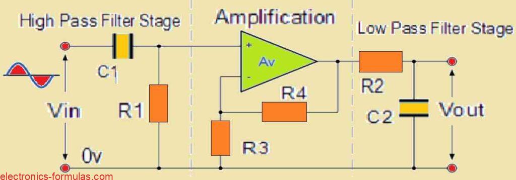
In this circuit we will cascade discrete passive low and high pass filters to produce a wide passband having a low Q-factor. The first stage functions as a high pass filter, using the capacitor to prevent any DC bias in the source signal.
This method generally has a significant advantage because of flat yet asymmetrical passband frequency response. In simple terms, one half of the reaction depicts the low-pass feature whereas the other half indicates the high-pass behavior. The diagram provided below might help you to understand this.

Now this is how we manage the corner frequencies or the cut-off frequencies in our cascaded system. We calculate the higher corner point (fH) and lower corner frequency cut-off point (fL), exactly like ordinary first-order low and high pass filters.
But there one thing we must remember! Maintaining a proper spacing between the two cut-off frequencies (fH and fL) is crucial. This separation eliminates cross-communication between the low and high pass stages, which we can accomplish by carefully selecting the components for the circuit.
The amplifier in the circuit serves a dual purpose. Firstly it isolates the cascaded low and high pass parts, preventing them from interfering with one another. Secondly it determines the total voltage gain of the filter which controls how much the signal is amplified.
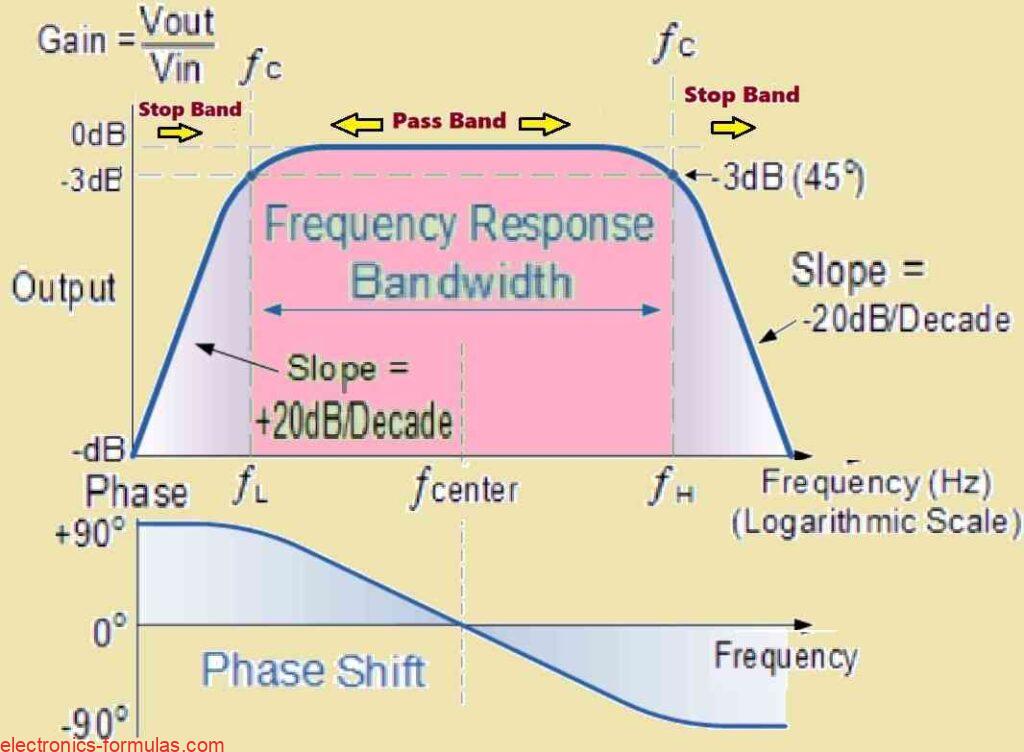
Now, let us discuss bandwidth. The bandwidth of the resultant band-pass filter is just the difference between the upper and lower -3dB values. For example if my filter had -3dB cut-off points at 200Hz and 600Hz, the bandwidth (BW) would be, BW = 600Hz – 200Hz = 400Hz.
Next, we will look at the normalized frequency response and phase shift characteristics of this active band-pass filter. This will give us a better grasp of how the filter performs at various frequencies.
Frequency Response Curve of an Active Band Pass Filter Circuit

The above-mentioned passive tuned filter can be used as a band-pass filter; however, its passband (bandwidth) is frequently rather large, which may be problematic for applications that need isolation of narrow frequency bands. Active band-pass filters may be made using inverting operational amplifiers but a more refined filter circuit can be created by restructuring the resistor and capacitor combinations. The resultant active band-pass filter has lower and upper -3dB cutoff frequencies represented by fc1 and fc2, respectively.
Inverting Band Pass Filter Circuit

Voltage Gain = -R1/R2,
fC1 = 1/2πR1C1,
fC2 = 1/2πR2C2
The above shown inverting band-pass filter arrangement has a narrower passband than its passive equivalent. The filters center frequency and bandwidth are determined by R1, R2, C1, and C2, with the op-amp providing the output.
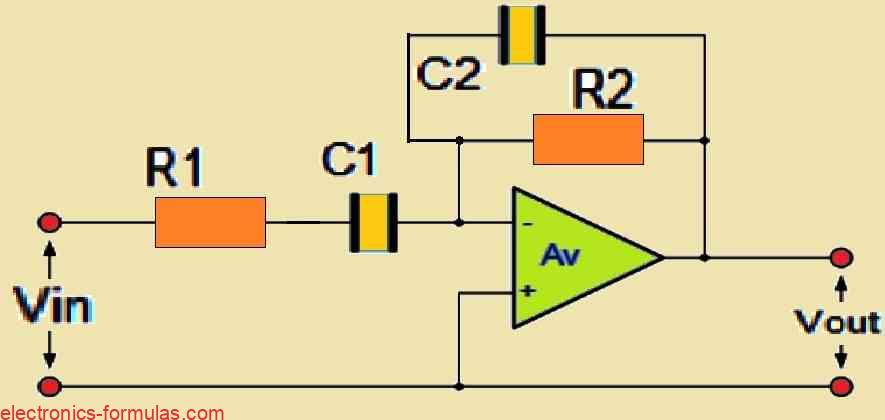
Infinite-Gain Multiple-Feedback (IGMF) Bandpass Filter
In order to achieve a more selective band-pass response, we use the IGMF topology. This active filter arrangement offers a high Q-factor and sharp roll-off characteristics that are centered around the resonant frequency (fr). The circuit outperforms the inverting design because of its intrinsic negative feedback mechanism.
This active band pass filter circuit takes advantage of the operational amplifier’s highest gain and applies multiple negative feedback via resistor R2 and capacitor C2. The IGMF filters characteristics may therefore be described using the formulas as follows:
fr = 1/2π[√(R1R2C1C2)]
QBP = fr/BW(3dB) = 1/2[√(R2/R1)]
Maximum Gain (Av) = -R2/2R1 = -2Q2
The relationship between resistors R1 and R2 determines the band-pass filter’s Q-factor and the maximum amplitude frequency. The circuit’s gain is represented as -2Q2. This shows that an increasing gain corresponds to an increasing selectivity, which indicates a narrower bandwidth.
Solving an Active Band Pass Filter Circuit Problem#1
Design an infinite-gain multiple-feedback band-pass filter with a unity voltage gain (Av = 1) and a resonant frequency (fr) of 10 kHz. Determine the necessary component values for circuit implementation.
To begin, we can calculate the values of the two resistors, R1 and R2, necessary for the active filter by utilizing the circuit’s gain to calculate Q, as explained below:
Av = 1 = -2Q2
∴ QBP = √(1/2) = 0.7071
∴ Q = 0.07071 = 1/2[√(R2/R1)]
∴ R2/R1 = [0.07071/(1/2)]2 = 2
From the above calculations we can see that with value of Q = 0.7071 there is a corresponding relationship where the resistor R2 becomes twice the value of resistor R1. Therefore, now we can choose some random appropriate values of resistances for the ratio of R2/R1. Let’s say resistor R1 = 12kΩ and R2 = 22kΩ.
In our problem, we know that the resonant frequency is 10kHz. By incorporating the above resistor values, we can quickly calculate the values of the capacitors required with the information in hand that C = C1 = C2.
fr = 10,000 Hz = 1/2 * π * C(√R1 * R2)
∴ C = 1/2 * π * fr (√R1 * R2)
= 1/[2 * π * 10000(√12000 * 22000)]
= 0.97953096 nF or simply 1 nF, which is the nearest standard value.
Resonant Frequency Point
The circuit characteristics of an active or passive band-pass filter determine its frequency response curve and the optimal response has a symmetrical passband. An active band-pass filter functions as a second-order filter because it has two reactive components using capacitors which causes the peak response to occur at the center frequency fc and resonant frequency fr. We can use the geometric mean of the lower fL and higher fH (-3dB) cutoff frequencies to calculate the center frequency, which is:
fr = √(fL * fH)
- In the above formula
- fr represents the resonant frequency or Center Frequency
- fL denotes the lower -3dB cut-off frequency point
- fH stands for the upper -3db cut-off frequency point
In our above explained problem#1, if we assume the lower and upper -3dB cut-off frequency points to 250Hz and 625Hz respectively, then we can calculate the resonant center frequency of the active band pass filter in the following manner:
fr = √(fL * fH)
= √(250 * 625)
= 395.28 Hertz
Understanding the Q Factor or the Quality Factor
One important factor in band pass filters is the Q Factor which measures how selective or non-selective the filter is throughout a certain frequency range.
The Q Factor specifically describes the width of the pass band between the upper and lower -3 dB cut-off frequencies of the filter
A lower Q factor indicates a wider bandwidth for the filter, meaning the filter enables a wider range of frequencies to pass through.
On the other hand a higher Q factor contributes to a narrower bandwidth which increases the selectivity of the filter, allowing only a certain range of frequencies to pass.
The Q Factor is commonly represented by the Greek letter a (alpha) which refers to the alpha-peak frequency as follows:
a = 1/Q
The alpha-peak frequency (a) plays a crucial role in the response curve of the filter.
The Q Factor of an active band pass filter (second-order system) is strongly related to the behavior of the filter around its center resonant frequency (fr).
Consider the Q Factor as the measure of the filters “sharpness” or “selectivity.”
It is also known as the “damping factor” or “damping coefficient.”
More amount of damping produces a flatter response curve.
Less amount of damping produces a sharper reaction.
The damping ratio (denoted by the Greek letter ξ) is related to the Q Factor as given below:
ξ = a/2
The Q factor or the “Q” of a band pass filter is the ratio of the Resonant Frequency fr to the Bandwidth BW across the upper and lower -3dB frequencies which we can see as given in the following image:

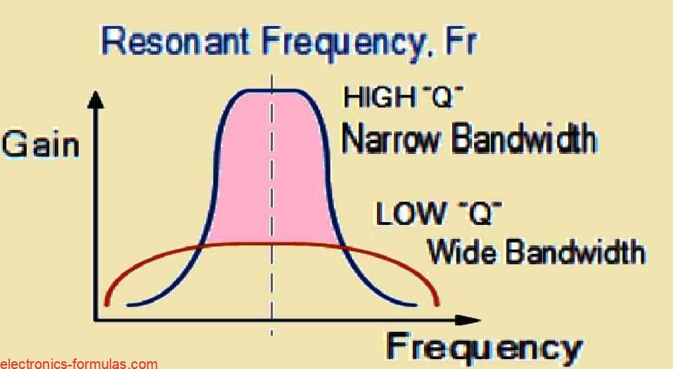
Q = Resonant Frequency/Bandwidth
Therefore, in our previously discussed problem, if we consider the bandwidth (BW) to 375Hz, which refers to the result of ƒH – fL, and the center resonant frequency, fr which we calculated to be 395.28 Hz, then the quality factor “Q” of the band pass filter can be calculated as:
375/395.28 = 0.94
As we can see the 0.94 does not have any units because Q is a ratio.
The Ideal Filter: A Conceptual Structure
In the field of theoretical circuit analysis, engineers frequently struggle to define what an ideal filter is. The perfectly flat passband of this hypothetical filter permits any frequencies lying inside a certain range to go through without restriction. On the other hand, its stopband is flawless as well, totally attenuating all frequencies that are not inside the intended passband. Like a sheer cliff, the transition between these two areas happens instantly.
Although it’s a useful conceptual tool, this ideal filter is entirely mathematical in nature. Such sudden shifts are literally impossible in the actual world of electrical components. We can only approximate this ideal behavior as best we can.
Using the Butterworth Approximation as a Workable Solutions
Now let’s put the Butterworth filter in place. Developing a filter design process like this is a big step toward creating a filter that nearly resembles the optimal response. Thanks to its’maximally flat’ passband feature, the Butterworth approximation is widely known. This indicates that the filters gain, or attenuation, is as constant as it may be over the whole passband.
The Butterworth filter, in comparison to other filter types, compromises some of the steepness of the transition between the passband and stopband in order to attain this flatness. This trade-off is frequently justified, though, as the flat passband is essential for many applications where the least amount of signal distortion is required.
Superior quality, Although it comes with more circuit complexity, Butterworth filters may be made to have higher roll-off rates in the stopband. Achieving the desired filter characteristics while taking into account the practical limitations of noise, power consumption, and component tolerances is where the art and science of filter design come into play.
Basically the Butterworth filter provides a decent transition into the stopband and a nearly perfect flat passband, with a mathematically valid and practical design method. It is the mainstay of analog filter design and a crucial equipment in the engineer’s toolbox.
References: Active Band Pass Filter Circuit
Designing an active bandpass filter and selecting R and C values