
So here we are talking about one more type of BJT amplifier, that is called Common Collector Amplifier. In this type of connection we give the input signal to the base pin of the transistor and then we take the output signal from the emitter pin. That means here the collector pin is working like a common point for both input side and output side.
That is why we call this setup as Common Collector or CC type because the collector pin is kind of grounded or earthed, mostly through the power supply side. So this collector pin becomes a shared path or common path.
Now if we compare this CC type with the famous Common Emitter (CE) type amplifier, then we will see both are opposite in many ways. In CE type we normally connect the load resistor at the collector side and we call that one RC. But in this CC type, we move that load resistor to the emitter side and now we call that as RE.
So this Common Collector or sometimes people call it Grounded Collector configuration, we mostly use it in those places where we have to join a high impedance signal source with a low impedance load at the output side but we also want high current gain in that case.
Now just see the basic Common Collector amplifier diagram given below, to understand it more clearly.
Common Collector Amplifier Circuit using NPN BJT

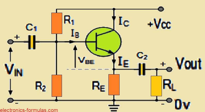
So here we are using two resistors R1 and R2 and we are connecting them in a way that they make a simple voltage divider circuit. This voltage divider is used for giving a fixed bias voltage to the base pin of the NPN transistor so that the transistor can start conducting properly.
Now this voltage divider network does not pull too much current from the transistor base so it is called a light loading. Because of that, we can easily calculate the base voltage VB, by using that normal voltage divider formula. That basic formula is shown below and it gives us the value of VB very quickly.
Understanding Voltage divider Network Circuits


So in this Common Collector (CC) amplifier setup, we are connecting the collector pin of the transistor directly to the supply voltage side which we call VCC. And here we are not putting any resistor at the collector side, that means RC = 0. So now when the transistor allows some collector current to flow, then that current creates a voltage drop across the emitter resistor, which is RE.
But in this CC type amplifier, this same voltage drop across RE which we call VE is also working like the output voltage. That means VOUT = VE here.
Setting the Output Voltage at Midpoint
Ideally what we want is to make the DC voltage across RE equal to half of the total supply voltage, that is VCC. Why?
Because then the transistor’s output voltage at no signal condition (we call that quiescent point) will sit exactly in the center of the working range. That helps the amplifier to give full swing of the output signal without any clipping from top or bottom side.
So to fix this midpoint condition, we must choose the RE value carefully. That value depends on how much base current IB is flowing and also the transistors current gain Beta or β.
How the Transistor Starts Conducting
Now we know that the base-emitter junction of the transistor is a PN-junction and it is forward biased in this case. So the base current starts flowing through it and reaches the emitter side.
This base current turns on the transistor and because of this, a much bigger current starts flowing from collector to emitter, which we call collector current IC.
So we can say the total current coming out of the emitter which is IE, is just the sum of IB and IC. That means:
IE = IB + IC
But practically, the base current is very small compared to collector current. So we can almost say:
IE ≈ IC
Input and Output Signal Connections
Just like in common emitter amplifier, here also we give the input signal to the base terminal of the transistor. But we already saw before that we take the output signal from the emitter pin, not from collector.
And now since the base and emitter pins are connected through only one forward biased PN-junction, so the input signal which we give to base, passes easily through this junction to the emitter. So the signal that comes out from emitter is in-phase with the input signal.
Why is it Called Emitter Follower
Because the output signal is coming from the emitter side and this emitter voltage just follows the input voltage applied at base (with only 0.7V drop), this type of amplifier is also known as Emitter Follower.
That means if input goes up, output also goes up following it and if input goes down, then output also goes down but always staying around 0.7V less than input (because of VBE drop).
So input and output signals are in-phase here and we say there is zero phase shift between VIN and VOUT.
Small Signal Resistance of the Emitter Junction
Now let us talk about the internal resistance of this forward biased base-emitter junction. Actually this junction behaves like a forward biased diode. So for small AC signals, this junction shows a small resistance which we call r’e (r-e prime). The formula to find this is:
r’e = 25mV / Ie
Here 25mV is called thermal voltage of the PN junction at normal room temperature (25°C) and Ie is the emitter current.
So as we increase the emitter current, then r’e value decreases.
Voltage Divider Effect and Voltage Gain
Now we must remember one thing. The base current flows through this small r’e resistance inside and then it also flows through the external emitter resistor RE which we connected outside. So these two resistors are in series and they form a small voltage divider.
Since r’e is very small and RE is very big (normally in kΩ), so the voltage drop mainly happens across RE. But because of this voltage divider action, the final output voltage becomes slightly less than the input voltage.
Output Voltage is Almost Equal to Input
Even though we are saying output voltage is less but actually the difference is very small. The output voltage swing (peak-to-peak) is almost 98% or 99% same as the input voltage. So most of the time we can say the voltage gain is almost 1, which is called unity gain.
Common Collector Amplifier Voltage Gain Formula
If we want to calculate the exact voltage gain which we write as VA, then we can use the voltage divider formula. In that we consider the base voltage VB as the input voltage VIN.
We already saw that output voltage VOUT comes across the RE resistor. And the input signal is applied across r’e + RE.
So voltage gain AV is calculated like this:
VOUT = VIN × RE / (r’e + RE)
So,
AV = VOUT / VIN
AV = (Ie × RE) / [Ie × (r’e + RE)]
AV = RE / (r’e + RE)
Now, we know that RE is much-much bigger than r’e. So we can say:
r’e + RE ≈ RE
So finally:
AV = RE / RE = 1
That means the voltage gain AV is approximately 1.
Why Common Collector Cannot Amplify Voltage
Here we see that this Common Collector amplifier setup, it cannot increase or boost the input voltage level. That means whatever input AC signal we apply at the base pin we get almost same voltage at the emitter pin, just around 0.7V lower because of that base-emitter junction drop.
So there is no voltage amplification happening here. That is why people also call this type of amplifier a Voltage Follower Circuit. Because whatever input voltage we give, the output voltage just follows it exactly without changing the level.
Output is in-phase with Input
Also the output signal which we get from the emitter is not inverted. It is fully in-phase with the input. That means both rise and fall together, no 180 degree shift like in common emitter amplifier.
So this CC circuit or emitter follower acts like a non-inverting amplifier.
Voltage Gain is Almost Unity
Because of all these reasons, we find that this circuit gives voltage gain very close to 1. That means output voltage is almost equal to input voltage. So we can say it is a unity gain amplifier and it does not amplify the voltage signal.
Solving a Common Collector Amplifier Circuit Problem #1
Given:
We have a common collector amplifier using NPN BJT and voltage divider bias. Here are the given values:
- Supply voltage VCC = 12V
- R1 = 5.5k = 5500 ohm
- R2 = 6.3k = 6300 ohm
- Load resistance RL = 4.3k = 4300 ohm
- Let us assume base-emitter voltage drop VBE = 0.7V
- Assume Beta = 100 (typical for small signal NPN BJT)
- Assume room temperature, so thermal voltage VT = 25mV = 0.025V
Step 1: Calculate VB (Base Voltage)
We will calculate base voltage VB using voltage divider formula:
VB = VCC × R2 / (R1 + R2)
= 12 × 6300 / (5500 + 6300)
= 12 × 6300 / 11800
= 12 × 0.5339
= 6.41V
So VB = 6.41V
Step 2: Calculate VE (Emitter Voltage)
We know that:
VE = VB – VBE
= 6.41 – 0.7
= 5.71V
So VE = 5.71V
VCE = VCC – VE
= 12 – 5.71
= 6.3V
Step 3: Calculate VC (Collector Voltage)
Since this is common collector amplifier, collector is directly connected to VCC and there is no RC resistor.
So:
VC = VCC = 12V
Step 4: Calculate IE (Emitter Current)
We will use Ohms law here. Load resistor RL is used at emitter side, so we use:
IE = VE / RL
= 5.71 / 4300
= 0.001327A
= 1.33mA
So IE = 1.33mA
Step 5: Calculate r’e (Internal Emitter Resistance)
We use:
r’e = VT / IE
= 0.025 / 0.00133
= 18.80 ohm
So r’e = 18.8Ω
Step 6: Calculate Voltage Gain AV
AV = RL / (r’e + RL)
= 4300 / (18.8 + 4300)
= 4300 / 4318.8
= 0.9957
So AV = 0.996
This is almost equal to , so confirming CC amplifier has unity voltage gain.
Final Answer:
| Parameter | Value |
|---|---|
| VB | 6.41V |
| VE | 5.71V |
| VC | 12V |
| IE | 1.33mA |
| r’e | 18.8Ω |
| AV | 0.996 (≈ 1) |
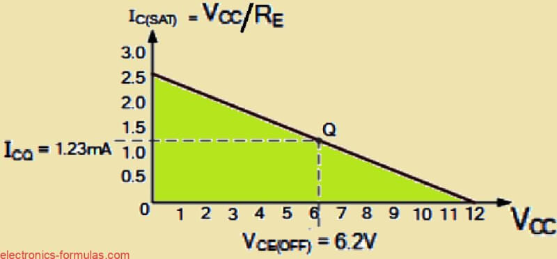
Final Common Collector BJT Amplifier Circuit with Load Line using the above Information


What is BJT Common Collector Input Impedance
So now we are talking about that common collector amplifier, right. That one also we call emitter follower. Now this one is not very great for voltage amplification because when we check that small signal voltage gain, it comes out to be nearly equal to 1 only. We write that like AV ≅ 1. So that means voltage goes in and comes out nearly same, no big increase.
But still we like this common collector circuit very much because it gives us one nice thing it works super good as voltage buffer.
Why that happens? Because this circuit gives us high input impedance, which we say ZIN and low output impedance which we say ZOUT. So what that does is, it separates or isolates our input signal source from the output load impedance. That means load cannot affect our signal source, because buffer is standing in the middle.
Now one more good thing is there in this circuit. That is, it gives current gain also which we write as Ai. As long as transistor is conducting properly, we get this current gain.
That means when small current goes inside base, which we call IB then this circuit allows a much bigger current to flow from collector to emitter. So small base current makes large emitter current, that is called current amplification.
And also remember, in this common collector circuit, we do not have RC resistor. Only RE is there which is emitter resistor. So that means DC current flowing through the transistor only sees RE in its path.
Then if we think about DC operating condition, that current becomes simply VCC divided by RE. So if RE is small then that current becomes big.
Now let us see this basic circuit diagram of common collector amplifier or emitter follower below:

So now we are trying to understand how this common collector amplifier behaves when we send small AC signal inside. For that, we have to do small signal AC analysis. In this method we treat all those capacitors like short wires because for AC signal they act like short circuit.
Also we short that VCC supply to ground because it has zero AC impedance. So basically we make a simplified version of the original circuit, which is called equivalent AC model.
Now in this equivalent model, we show all the voltages and currents related to biasing and small signal. That helps us to understand how the AC signal flows and what gain or impedance we get.

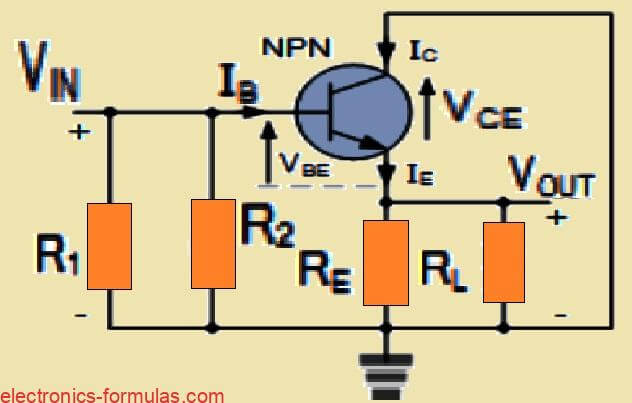
RB = R1 parallel R2
Re = RE parallel RL
β = IC / IB ⇒ IC = β × IB
Since IE ≈ IC, then:
IE ≈ IC = β × IB
VIN = VB = VBE + VE
So now the input impedance (ZIN) which we see when we look inside the base terminal of this common collector configuration, is given as:
So now what we do here…
We already saw earlier that to find the input impedance of common collector amplifier we need to calculate the impedance looking into the base. That means we got:
ZIN = RBIAS parallel Zbase
Where:
Zbase = Vb / Ib
But now we go deeper and break down that Zbase thing using ohm’s law and transistor current relations.
Now here is what happens:
We know:
Vb = ie × (Re + r’e)
Because base voltage is across the emitter branch (Re + re) multiplied by total emitter current (ie)
Also we know:
ie = ic + ib
And
ic = β × ib
So we put these values inside Vb/Ib and we get:
Rewriting All Equations in Plain Text:
ZIN = RBIAS parallel Zbase
Zbase = Vb / Ib
Vb = ie × (Re + r’e)
ie = ic + ib
ic = β × ib
So, ie = β × ib + ib = ib × (β + 1)
Now,
Zbase = Vb / Ib = ie × (Re + r’e) / Ib
= [(β + 1) × Ib × (Re + r’e)] / Ib
= (β + 1) × (Re + r’e)
So final expression becomes:
Zbase = (β + 1) × (Re + r’e)
But then we know that β is usually a big number like 100 or more, so adding 1 does not change it much. So we can simply write:
Zbase ≈ β × (Re + r’e)
So what this tells us is simple. When we try to inject AC signal from the base side, the impedance we see is actually very high because the emitter side impedance gets multiplied by beta. Thats why common collector is called a buffer stage, it gives high input impedance and low output impedance.
Final Base Impedance Formula (super simplified):
Zbase = β × (Re + r’e)
Where:
β is the transistor’s current gain. It means how many times the base current is amplified to make the collector current.
Re is the AC emitter resistance that we usually put as a resistor in series with the emitter pin.
r’e is the internal ac resistance of the base-emitter diode, like the small dynamic resistance inside the transistor. This is usually just a few ohms (around 25mV/Ie).
But then…
Re is usually in kilo-ohms and r’e is just few ohms, so Re >> r’e.
So when we add them:
Re + r’e ≈ Re only
That means, the base impedance becomes:
Zbase ≈ β × Re
So what is the point here?
We understand that this base impedance (Zbase) is directly linked to the emitter resistor. So if we increase or decrease Re, then base impedance also increases or decreases, multiplied by β.
Now here comes one interesting point:
In many circuits, we do not have only Re, there may be a load resistor RL connected too, either to emitter or as part of the output.
And in many situations, Re and RL may be parallel to each other from the AC point of view.
So:
Zbase = β × (Re parallel RL)
Which means:
Zbase = β × (Re // RL)
(where // means parallel combination)
So this base impedance value can be controlled or changed by adjusting Re or RL, because they both affect the emitter side resistance seen by the base.
But wait bro, one more thing…
This Zbase that we calculated is the impedance looking into the base only, like if we zoom into the transistor only then.
But in real amplifier, the input signal comes through a bias network — usually there are two resistors making a voltage divider to bias the base. These resistors are:
R1 from Vcc to base
R2 from base to ground
Together they form a parallel impedance called RBIAS, so the true input impedance seen by the signal source is:
Final Input Impedance of Amplifier:
ZIN = RBIAS // Zbase
Where:
RBIAS = R1 // R2
Zbase = β × (Re + r’e) or just β × Re (if re is very small)
So this is what the signal source will actually see when we connect it to the amplifier input.
Solving another Common Collector Amplifier Circuit Problem #2
Now let us take that same previous common collector amplifier circuit which we already saw above and calculate the input impedance at the base of the transistor and also the full input impedance of the amplifier stage, and let take all the above given values, right? Also let us assume the load resistance RL is 10k ohm and the current gain of the NPN transistor, that is hFE or beta, is given as 100.
Step 1: First calculate the base input impedance of the transistor which is called Zbase.
We use the formula:
Zbase = beta × (Re + r’e)
Here:
beta = 100
Re = RL = 4300 ohm
r’e = 18.8 ohm
So:
Zbase = 100 × (4300 + 18.8)
Zbase = 100 × 4318.8
Zbase = 431880 ohm
Therefore Zbase is equal to 431.88 kilo ohm
Step 2: Now calculate the equivalent resistance of the bias divider network, made by R1 and R2
We use the formula:
RBIAS = (R1 × R2) / (R1 + R2)
Here:
R1 = 5500 ohm
R2 = 6300 ohm
So:
RBIAS = (5500 × 6300) / (5500 + 6300)
RBIAS = 34650000 / 11800
RBIAS = 2936.44 ohm
Therefore RBIAS is approximately equal to 2.94 kilo ohm
Step 3: Now calculate the total input impedance of the amplifier stage called ZIN
We do this by calculating the parallel of Zbase and RBIAS:
ZIN = (Zbase × RBIAS) / (Zbase + RBIAS)
Substituting the values:
ZIN = (431880 × 2936.44) / (431880 + 2936.44)
ZIN = 126805459.2 / 434816.44
ZIN = 2916.25 ohm
Therefore the input impedance of the amplifier stage is around 2.92 kilo ohm
Final Summary:
| Parameter | Value |
|---|---|
| Zbase | 431.88 kΩ |
| RBIAS (R1 // R2) | 2.94 kΩ |
| Input Impedance ZIN | ≈ 2.92 kΩ |
So here, we can see that the transistors base impedance is around 432k ohm, right, but the total input impedance of the full amplifier is coming only around 3k ohm or like that. That means this Zbase value is actually much-much higher than ZIN.
Because of this big difference, we can say that the actual input impedance of the common collector amplifier stage is not getting decided by this big Zbase, but it is mainly getting fixed or controlled by that R1 and R2 resistors, which are making the voltage divider bias network. So finally we say that this amplifier’s input impedance is mostly equal to the parallel value of R1 and R2 only.
Calculating Collector Output Impedance
Now if we want to calculate the collector output impedance or basically the ZOUT of this common collector amplifier stage then first what we have to do is — we have to imagine that the load is removed.

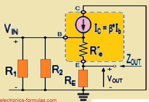
Because we are not interested in the load here but we want to find out how much resistance this amplifier itself is offering to that load, right. So that means we have to see from the load side and try to look back inside the amplifier from the emitter terminal, that what resistance is appearing there.
Now when we do this, we must consider the internal impedance of the transistor also and the way the base is connected through the biasing resistors. So we take the equivalent AC circuit and we use the formula like this:
ZOUT = RE parallel with (r’e + (R1 parallel R2) divided by (beta + 1))
That means ZOUT = RE || (r’e + (R1 || R2) / (β + 1))
Here RE is that actual emitter resistor r’e is the small signal resistance inside the transistor and R1 || R2 is the parallel value of the voltage divider resistors from the base side. Then we divide that by beta plus 1 because of the way the current gain reflects the impedance from base to emitter side.
Now if we take all the actual values from our earlier calculations and we put them inside this formula, then we will get ZOUT as around 49.5 ohm which is really small compared to the input impedance from base side, which we saw was like in kilo ohms, right.
So finally we can say that this common collector amplifier is having one really high input impedance and one very low output impedance.
That means it is good for connecting a high impedance signal source on input and then driving a low impedance load on output side. This is the reason why we mostly use this CC amplifier as a kind of buffer amplifier, where we need unity gain but proper impedance matching from input to output.
So now after we already found that our amplifiers output impedance ZOUT is coming close to around 50 ohm by calculation, we can go to the next step.
That is, we now connect back that 10k ohm load resistor again to the output of this common collector amplifier circuit. Then we try to find out what is the new or final output impedance after including that load.
So to calculate this, we simply take ZOUT in parallel with RL. That is:
ZOUT(LOAD) = ZOUT || RL = (49.5 × 10000) / (49.5 + 10000) = around 49.3 ohm…
So even though this load resistor RL is quite high, like 10k ohm, still when we connect it, then final output impedance becomes around 49.3 ohm only which is still very low.
Why this is happening? That is because this RL is very big compared to ZOUT. So in parallel formula, the smaller value dominates. And also if we want to get maximum power transfer to the load, then that load resistance RL should match the source impedance, which is ZOUT in our case.
We also know that the voltage gain of a CC amplifier is basically unity, that means 1. So voltage does not increase or decrease, it just follows input. But even if voltage gain is 1, then power gain can still be there. That power gain will then be equal to current gain only, because P = V × I.
Then we also know that in this common collector setup, the current gain is decided by the ratio of emitter current to base current. That is IE / IB, and this value is equal to beta + 1.
Finally we can say that the current gain of this amplifier is almost equal to beta… because adding 1 to beta does not change it much.
So the overall current gain of the amplifier is same as transistor’s beta and because voltage gain is 1, the power gain is also same as beta.