
When we talk about the common source JFET amplifier, there is this really cool advantage that it has over the common-emitter BJT amplifier.
The big deal here is that the Field Effect Transistor or FET for short, boasts an incredibly high input impedance. This means it can handle very tiny input voltage signals without breaking a sweat.
Plus, it produces a low noise output, which makes it just perfect for those amplifier circuits that need to work with really small signals.
Now in the world of transistor amplifier circuits, we often find ourselves using Bipolar Transistors, especially in setups like the common emitter amplifier.
However it is worth mentioning that we can also create small signal amplifiers using Field Effect Transistors.
The whole idea behind designing an amplifier circuit that revolves around a junction field effect transistor which we are calling “JFET” here (and specifically looking at the N-channel FET for this tutorial) or even a metal oxide silicon FET—also known as “MOSFET”—is fundamentally based on the same principles we discussed when we explored the bipolar transistor circuit used in a Class-A amplifier circuit in our previous tutorial.
To get started with this, the very first thing we need to do is identify a suitable quiescent point which is often referred to as the “Q-point.”
This step is crucial because it allows us to properly bias the JFET amplifier circuit. When working with single amplifier configurations like Common-source (CS), Common-drain (CD), or Source-follower (SF), as well as Common-gate (CG), these configurations are generally available for most FET devices.
The common-emitter, emitter-follower, and common-base arrangements utilizing bipolar transistors are represented by these three JFET amplifier configurations. Since the Common Source JFET amplifier is the most extensively used JFET amplifier design, we will focus on it in this FET amplifier lesson.
Let’s discuss the circuit schematic for the Common Source JFET Amplifier as shown hereunder.
Analyzing the Common Source JFET Amplifier Circuit

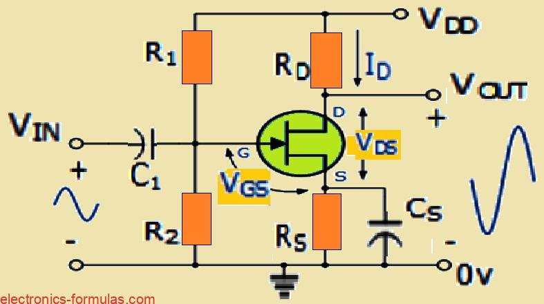
So when we talk about this amplifier circuit, it is built around an N-channel JFET, which is a type of field-effect transistor.
However you should know that you could totally swap this out for an equivalent N-channel depletion-mode MOSFET.
The cool thing is that if you did that, the circuit diagram would not change at all, it would just be a different kind of FET in the same setup. This circuit is arranged in a common source configuration is actually pretty standard for amplifiers.
Now let us discuss how the gate voltage Vg for the JFET gets its biasing. This is done through a potential divider network that is created using two resistors R1 and R2.
The purpose of this biasing is to make sure that the JFET operates within its saturation region. This saturation region is actually similar to what we refer to as the active region in bipolar junction transistors (BJTs).
One major difference between this JFET setup and a typical bipolar transistor circuit is that the junction FET does not draw much input gate current at all.
Because of this characteristic we can treat the gate as if it were an open circuit.
This means that we do not need to worry about input characteristic curves like we would with other types of transistors.
To help you illustrate these differences more clearly we can look at a comparison between the JFET and the bipolar junction transistor (BJT) in the table below.
JFET vs Bipolar Junction Transistor (BJT) Table
| Junction FET | Bipolar Transistor |
| Gate, ( G ) | Base, ( B ) |
| Drain, ( D ) | Collector, ( C ) |
| Source, ( S ) | Emitter, ( E ) |
| Gate Supply, ( VG ) | Base Supply, ( VB ) |
| Drain Supply, ( VDD ) | Collector Supply, ( VCC ) |
| Drain Current, ( ID ) | Collector Current, ( IC ) |
Now, talking about the N-Channel JFET, this particular type of JFET is what we call a depletion mode device which basically means that it is normally always in an “ON” state.
To control or modulate the drain current flowing through it, you need to apply a negative gate voltage in relation to the source.
You can achieve this negative voltage by either using a separate power supply or by setting up a self-biasing arrangement.
The important thing is that there needs to be a steady current flowing through the JFET, even when there is no input signal coming in.
This ensures that the gate-source pn junction remains in reverse bias.
In our straightforward example we are using a potential divider network to provide the necessary biasing.
This setup allows the input signal to create both a voltage drop and a voltage rise at the gate when you have a sinusoidal signal coming in.
You can use any suitable combination of resistor values, as long as they are in the right proportions to generate the correct biasing voltage.
So the DC gate biasing voltage Vg, can be expressed using the following formula:
VG = (VDD * R2)/ (R1 + R2)
VDD = (R2 / R1 + R2)
Just to clarify, this equation is really only about figuring out the ratio between the two resistors R1 and R2.
However if we want to really make the most of the super high input impedance that the JFET offers and also keep the power dissipation in the circuit to a minimum, we should aim to make these resistor values as high as we can.
Typically you will find that values around 1MΩ to 10MΩ are pretty common and work well.
Now let us talk about the input signal which is referred to as Vin in the context of a common source JFET amplifier.
This input signal is applied between the Gate terminal and what we call the zero volts rail, or 0V for short.
When we have a steady value of gate voltage denote as Vg, applied to the JFET, it operates in what is known as its “Ohmic region.”
In this region it behaves like a linear resistive device which is pretty handy.
Moving on to the drain circuit, it contains something called the load resistor Rd.
The output voltage Vout, is developed across this load resistance.
If we want to boost the efficiency of our common source JFET amplifier even more, we can add in a resistor called Rs.
This resistor is placed in the source lead and allows the same drain current to flow through it.
Additionally resistor Rs plays an important role in setting what is known as the JFET amplifier’s “Q-point” which is crucial for its operation.
Whenever we turn ON the JFET fully “ON,” a voltage drop that is equal to Rs multiplied by Id develops across this resistor.
This situation pulls up the potential of the source terminal above 0V, which is also referred to as ground level.
The voltage drop that occurs across Rs, caused by the drain current creates the necessary reverse biasing condition across the gate resistor R2.
This effectively generates what we call negative feedback which is quite important in this context.
Now in order to maintain that reverse bias at the gate-source junction, it is essential for the source voltage Vs, to be higher than the gate voltage Vg.
So we can express this source voltage as follows:
VS = ID * RS = VG – VGS
When “No Current” reaches the gate terminal, the drain current Id is also equal to the source current Is, and may be expressed as follows:
ID = VS / RS = VDD / (RD + RS)
So this thing called a potential divider biasing circuit really helps to make the common source JFET amplifier work more smoothly when it is running off just one DC power supply.
This is different from using a fixed voltage biasing circuit which does not provide the same level of stability.
In this setup we have a resistor Rs, along with a source bypass capacitor known as Cs.
These components do jobs that are kind of like what you would find in a common emitter bipolar transistor amplifier where they help keep things stable and reduce any loss in voltage gain.
Now there is a bit of a trade-off here. To get that nice, steady quiescent gate voltage, we end up using up a larger chunk of the supply voltage across Rs.
It is like giving up some of the power to keep everything running smoothly.
When we look at the source bypass capacitor, it usually has a pretty high capacitance value—like over 100 µF—and it is polarized too.
This means it has a certain direction it needs to be connected in. Because of this characteristic, the impedance value ends up being really low—less than 10% of the transconductance (gm) of the device.
When we start working with higher frequencies, this bypass capacitor acts almost like a short circuit which means it connects the source straight to ground without any resistance getting in the way.
The common emitter amplifier and a common source JFET amplifier share much of the same fundamental circuitry and properties. Integrating the two points for the drain current Id, and the supply voltage Vdd, creates a DC load line.
Keep in mind that as long as Id = 0, Vdd = Vds, and when Vds = 0, then Id will be = Vdd/RL. Therefore as a result, the load line is the location where the curves connect at the Q-point.
Characteristics Curves for the Common Source JFET Amplifier Circuit

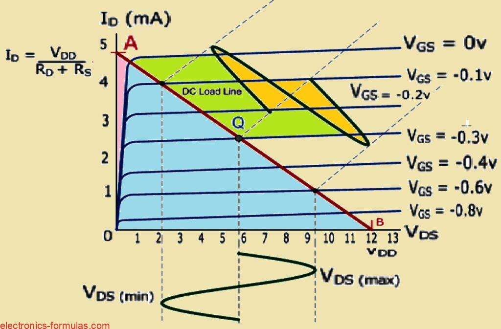
So just like what happens with the common emitter bipolar circuit, when we look at the DC load line for a common source JFET amplifier, we end up with this straight line equation.
The slope of this line or its gradient, is expressed as -1 divided by the sum of Rd and Rs. If you take a peek at the vertical Id axis you will notice that this line crosses at a point we can call point A which is calculated as Vdd divided by the total of Rd and Rs.
Now if you look at the other end of this load line, it makes contact with the horizontal axis at point B which simply equals the supply voltage Vdd.
When it comes to where the Q-point actually lands on this DC load line, it is typically found right in the middle of the load line (especially for class-A operation).
This positioning is influenced by the average value of Vg which is set to be negative, because remember, the JFET operates in depletion mode.
Just like with the bipolar common emitter amplifier, the output from our common source JFET amplifier flips 180 degrees out of phase compared to the input signal.
Now let us talk about one of the significant downsides of using depletion-mode JFETs: they require negative biasing.
If for some reason this bias were to fail—like something goes wrong—the gate-source voltage could end up rising and turning positive.
This would lead to an increase in drain current which could ultimately cause problems with the drain voltage Vd.
Additionally the junction FET has this high channel resistance Rds(on) and when you combine that with a high quiescent steady-state drain current, it causes these devices to generate quite a bit of heat.
Because of this heat generation you will definitely need to add a heatsink to keep things cool.
On the bright side many of the issues that come with using JFETs can be significantly minimized if you opt for enhancement-mode MOSFET devices instead.
Now speaking of MOSFETs which stands for Metal Oxide Semiconductor FETs, these guys come with much higher input impedances and lower channel resistances when you compare them to their JFET counterparts.
Another thing to keep in mind is that the biasing setups for MOSFETs are a bit different.
If we do not apply positive bias for N-channel devices and negative bias for P-channel devices then we will not see any drain current flowing at all.
This essentially means we have what you could call a fail-proof transistor, which is pretty neat…
Current and Power Gains of JFET Amplifier Circuits
Earlier we mentioned that the input current, which we refer to as Ig, in a common source JFET amplifier is really quite small.
This is largely due to the fact that the gate impedance, known as Rg is extremely high. Because of this characteristic, a common source JFET amplifier boasts an impressive ratio between its input and output impedances.
So for any given amount of output current which we call IOUT, the JFET amplifier will achieve a very high current gain, denoted as Ai.
This unique feature makes common source JFET amplifiers incredibly useful when it comes to impedance matching circuits or when they are utilized as voltage amplifiers.
Furthermore considering that power is calculated using the formula Power = Voltage * Current (which we can write as P = V * I) and since the output voltages typically range from several millivolts to even a few volts, it follows that the power gain, represented as Ap is also quite high.
References: