
Normally you will find a digital logic gate will accept multiple inputs, for example A, B, C, D, etc., but would mostly provide only one digital output, denoted as Q. We can connect or cascade multiple individual logic gates, to generate logic gate functions with any desired number of inputs, which can be used to design combinational and sequential circuits, or produce various logic functions from standard gates.
The digital logic gates that we get in the market, generally come in two main families: TTL (Transistor-Transistor Logic), exemplified by the 7400 series, and CMOS (Complementary Metal-Oxide-Silicon), represented by the 4000 series.
TTL and CMOS refer to the logic technology used in manufacturing these integrated circuits (ICs), often referred to as “chips.” TTL logic ICs typically use NPN and PNP bipolar junction transistors, while CMOS ICs use complementary MOSFET or JFET field-effect transistors for both input and output circuitry.
Apart from the TTL and CMOS technologies, we can also build digital logic gates by discrete components such as diodes, transistors, and resistors, to create in RTL (Resistor-Transistor Logic) gates, DTL (Diode-Transistor Logic) gates, or ECL (Emitter-Coupled Logic) gates.
However, you may see that these types of logic gates are less common today compared to the widely used CMOS family. We can classify the Integrated circuits (ICs) into logic families with regards to how many number of transistors or “gates” they contain.
For example a simple AND gate may use only a few transistors, but on the other hand a complex microprocessor chip may include billions of transistors on a single wafer.
We can categorize IC with respect to their number of logic gates used or the complexity of circuits within a single chip, with classifications based on the number of individual gates, as described below:
How Integrated Circuits or ICs are Classified
Small Scale Integration (SSI) – In this category we will see chips that accommodate up to 10 transistors or a few gates inside a single package, such as AND, OR, and NOT gates.
Medium Scale Integration (MSI) – The Chips that we include in this category may contain between 10 and 100 transistors or several tens of gates inside a single package. They are designed to handle digital operations such as adders, decoders, counters, flip-flops, and multiplexers.
Large Scale Integration (LSI) – In these chips they incorporate between 100 and 1,000 transistors or hundreds of gates. We can use these chips for specific digital operations which include I/O chips, memory, and arithmetic and logic units.
Very-Large Scale Integration (VLSI) – We find that VLSI chips contain between 1,000 and 10,000 transistors or thousands of gates, which can perform computational tasks such as processors, large memory arrays, and programmable logic devices.
Super-Large Scale Integration (SLSI) – Chips that fall this category feature between 10,000 and 100,000 transistors inside a single package. We can use these chips for implementing advanced computational operations like microprocessor chips, micro-controllers, basic PICs, and calculators.
Ultra-Large Scale Integration (ULSI) – These chips are built using more than 1 million transistors, and are the most complex with their design, and we can use them in high-performance applications such as computer CPUs, GPUs, video processors, micro-controllers, FPGAs, and complex PICs.
Although you may find that the “ultra large scale” (ULSI) classification are not much used, we find another level of integration that represents the complexity of an integrated circuit also known as the System-on-Chip (SoC).
In an SoC, you will see that individual components like the microprocessor, memory, peripherals, and I/O logic are all integrated onto a single piece of silicon, which effectively provides us with a complete electronic system inside just a single chip, embodying the concept of “integration” in integrated circuits.
These types of advanced integrated chips are able to accommodate as much as 100 million individual silicon-CMOS transistor gates inside a single package. We can typically see them being used in mobile phones, digital cameras, micro-controllers, PICs, and various robotic applications.
Moore’s Law
In the year 1965, Gordon Moore, who is known to be one of Intel’s co-founders, made an interesting prediction about semiconductor technology, he said that “the number of transistors and resistors on a single chip would double every 18 months.” During that time we had silicon chips which were designed with a maximum of around 60 individual transistor gates.
The Intel 4004 microprocessor which was first launched in the year 1971 to be the worlds first microprocessor, featured a 4-bit data bus that included about 2300 transistors, running at a speed of approximately 600 kHz.
If we now fast forward and come to 2023, we find that the Intel’s Quad-core i7-2700K Sandy Bridge 64-bit microprocessor clearly proving the reality of Moore’s prediction.
This modern microprocessor includes around a staggering 1.2 billion transistors and can operate with an astonishing rate of nearly 4 GHz. As we come across newer and faster microprocessors and micro-controllers, these continue to become more and more advanced with the transistor count on chips increasing day by day.
Logic States of Digital ICs
We can employ Digital logic gates as the fundamental elements from which we can build all digital electronic circuits and microprocessor-based systems. These basic gates can be used to implement logical operations, for example like AND, OR, and NOT on binary numbers.
While working with digital logic design, we find that only two voltage levels or states are allowed here, which are commonly called as Logic “1” and Logic “0,” or HIGH and LOW, or TRUE and FALSE. In Boolean Algebra and standard truth tables we represent these states through the binary digits “1” and “0,” respectively.
We can take a standard light switch as the straightforward example of a digital state. Here, we find two possible states for the switch: “ON” and “OFF”, which means it is simply not possible for this switch to occupy two states at any one time. We can better understand the idea of digital states and their binary nature with the help of the following table:
| Boolean Algebra | Boolean Logic | Voltage State |
| Logic “1” | TRUE (T) | HIGH (H) |
| Logic “0” | FALSE (F) | LOW (L) |
You will find that the majority of digital logic systems use “Positive logic,” in which a logic level “0” or “LOW” corresponds to zero voltage (0V) or ground, while a logic level “1” or “HIGH” denotes a higher value, such as +5 volts. The change that occurs between these voltage levels, whether from a logic level “0” to “1” or from “1” to “0”, is carried out with maximum speed to avoid any failure in the logic circuit.
On the other hand, we find that there is a “Negative Logic” system, which reverses the definitions and rules for logic levels “0” and “1”. However, in the following section on digital logic gates, we will concentrate on the positive logic conventions, as it is the most generally used.
Now, for common TTL (transistor-transistor logic) integrated circuits, specified voltage ranges are set for input and output levels, which clearly define what makes up a logic “1” and a logic “0.” You can see the detailed voltage ranges are described below.
Input and Output Voltage Levels of TTL ICs

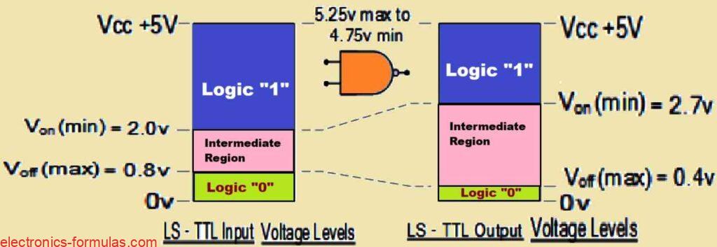
We can get digital logic gates of the bipolar 7400 and CMOS 4000 series in a variety of forms, such as 74Lxx, 74LSxx, 74ALSxx, 74HCxx, 74HCTxx, 74ACTxx, and more. Each variety has its own particular combination of benefits and downsides. Here we see that the precise voltage required to create a logic “0” or a logic “1” is different depending on the logic family or group.
TTL and CMOS Logic Voltage Levels
When we are working with a standard +5 volt power supply, any TTL voltage input ranging from 2.0 V to 5 V will be interpreted as a logic “1” or “HIGH,” whereas any input below 0.8V will be read as a logic “0” or “LOW.” The voltage range that lies between these two levels whether as an input or output, is referred to as the Indeterminate Region. If we operate the device within this region it can lead to the logic gate generating illegitimate outputs.
When we talk about the popular CMOS 4000 logic family, we find that these operates with different voltage levels compared to TTL types, mainly because these are built using field-effect transistors (FETs).
In CMOS technology, we define a logic “1” by a voltage range that can be anywhere between 3 V to 18 volts and a logic “0” can be mostly below the 1.5 volts level. In the table below we will witness the differentiations between the logic levels of conventional TTL and CMOS logic gates.
| IC Type | Logic 0 | Logic 1 |
| TTL | 0 to 0.8 V | 2.0 to 5 V (VCC) |
| CMOS | 0 to 1.5 V | 3.0 to 18 V (VDD) |
Digital Logic Gate Voltage Levels for Ideal TTL ICs
In accordance with the data explained above, we understand that an ideal TTL digital logic gate may be characterized as follows: it will have a “LOW” level logic (logic “0”) of 0 volts (ground) and a “HIGH” level logic “1” of +5 volts. This may be illustrated as follows.

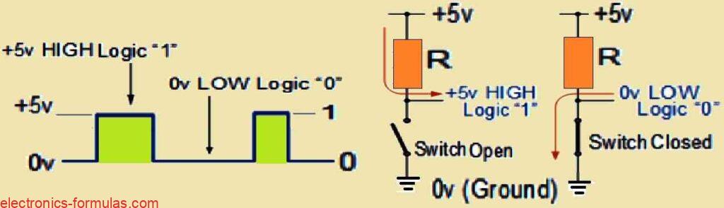
With reference to the above diagram we see that the opening or closing of the switch results in an either a logic level “1” or a logic level “0”. Here, the resistor R is implemented as a “pull-up” resistor.
In the range that lies between the clearly defined HIGH and LOW voltage levels, we face what is generally known as “no-man’s land” (seen in blue above). If we happen to apply a signal voltage that comes within this uncertain zone, we do not know whether the logic gate will read it as a “0” or a “1,” resulting in an unexpected output.
We call this unpredictable and undesired voltage that enters electrical circuits “noise.” Noise can be caused by external interferences such as adjacent switches, power supply oscillations, or stray electromagnetic radiation picked up by cables and other conductors. To ensure that our logic gate is not impacted by such noise, we need to have some kind of noise buffer or immunity.
Noise Immunity in Digital Logic Gate

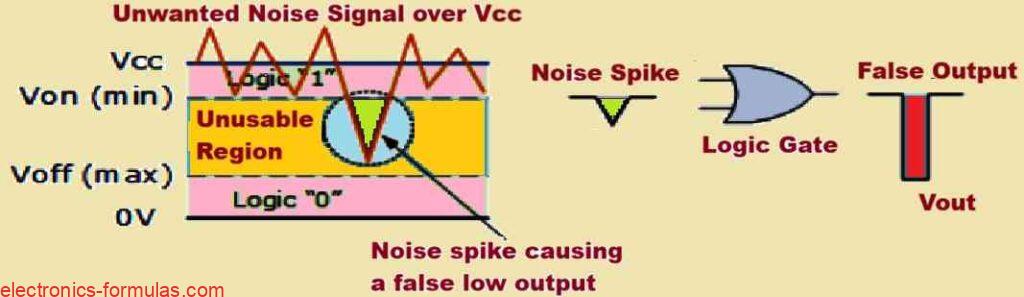
In the figure above we can see that the noise signal is riding on top of the Vcc supply voltage. So, as long as the noise is over the minimal threshold (VON(min)), the logic gate’s input and output stay stable.
But if the noise level rises sufficiently and a noise spike causes the HIGH voltage to drop below this minimal threshold, then the logic gate may misinterpret this spike as a LOW level input. This might cause the gate to emit a misleading signal as a result of an accidental switch.
To guarantee that a logic gate is not impacted by noise, we must design the circuit in such a way that it is able to resist a particular quantity of unwanted noise on its input without changing its output state.
Basic Digital Logic Gate Configurations
Interestingly it may be possible for us to create simple digital logic gates just by combining transistors or BJTs, diodes and resistors together.
A basic example of a Diode-Resistor Logic (DRL) can be seen in the figure given below.

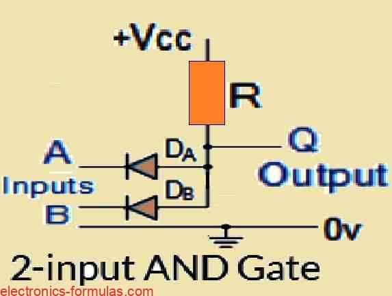
Also, you may find it easy to convert the above 2-input Diode-Resistor AND gate into a NAND gate. To do this we just have to add a single transistor configured as an inverter (NOT gate) to the existing circuit, as shown below:

The fact is that, the Diode-Resistor AND gate produces a high output only when both inputs are high, so by adding the inverter we flip this output turning it into a NAND gate, wherein the output is low only when both the inputs are high.
Drawbacks
In practice you may find that using discrete components such as diodes, resistors, and transistors for making digital logic gates may not be an ideal option for commercial applications.
Because we may encounter issues like propagation delay and gate delay, which might affect the speed of our circuits. Another thing is that, the pull-up resistors, although they are necessary might result in a power loss because they may continuously consume power.
There is one more challenge we might face if we employ a diode-resistor logic which is the lack of “Fan-out” capability. This means that we cannot use its one output to drive multiple inputs in subsequent stages effectively which might limit its use in complex circuits.
One more issue we may see is that this type of design does not fully turn off, as you may find that a Logic “0” still causes an output voltage of about 0.6V due to the diode’s internal voltage drop.
For these reasons, most of us might prefer using TTL (Transistor-Transistor Logic) and CMOS (Complementary Metal-Oxide-Semiconductor) technologies which provide us with better performance and clearer logic levels.
Basic TTL Logic Gate Configurations
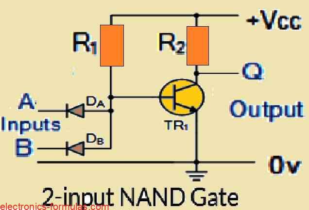
In the basic TTL setup discussed above, we start with a Diode-Resistor AND gate that uses separate diodes for each input.
Now, because all bipolar transistor regardless of whether it is a NPN (Negative-Positive-Negative) or PNP (Positive-Negative-Positive), incorporates two diode junctions connected together internally, we can simply replace these diodes with a single NPN transistor which can have multiple emitter terminals. This is the configuration what we call as TTL (Transistor-Transistor Logic).

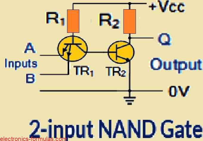
In our TTL NAND gate circuit we use an input transistor (TR1) with multiple emitters corresponding to inputs “A” and “B” and a single-stage inverting NPN switching transistor (TR2).
Lets understand how this might work:
When the Inputs Are LOW (0V): If we apply either or both emitters of TR1 with a logic level “0” signal, the base current of TR1 will flow through its base-emitter junction to ground (0V).
Because of this TR1 will saturate and its collector terminal will follow this ground level. Due to this the base of TR2 will get connected to ground (0V), turning TR2 “OFF.” Therefore this will cause the output at Q to be HIGH because TR2 is not conducting.
When the Inputs Are HIGH (Logic Level 1): If we apply both inputs “A” and “B” with a logic level “1” signal, TR1 will turn “OFF” because there is no base current. This will make the base of TR2 turn HIGH which will turn TR2 “ON” and finally the output at Q will become LOW due to the switching action of TR2.
So we find that by connecting multiple emitters to the inputs, TR1 allows the circuit to operate as a NAND gate where the output is LOW only when all inputs are HIGH. By using this simple setup it becomes possible for us to design and enhance the efficiency of digital circuits.
Emitter-Coupled Digital Logic Gate Configurations
When we talk about Emitter-Coupled Logic (ECL), we are primarily dealing with a type of digital logic gate that uses bipolar transistor logic in quite a distinct way.
Unlike standard TTL logic gates in which we find transistors operating in the saturation region, ECL transistors are never able to th reach saturation level, instead, here we configure the input and output circuits with push-pull connected transistors, and we set the supply voltage to be negative with regards to the ground.
When we use this type of configuration it allows ECL gates to operate at speeds up to the Gigahertz range which is much faster compared to standard TTL gates.
But, we surely need to be aware that ECL can be quickly affected by noise, simply because the unsaturated transistors operate within their active region, in which they both work by amplifying and switching the signals, and this can make the noise very very significant issue in ECL logic.
Sub-families of Integrated Circuits having the “74” Prefix
When we see the digital ICs starting with the “74” series, it represents a range of TTL bipolar transistor technology that are specifically designed to tackle factors like propagation delays, current consumption, and fan-in and fan-out requirements. In this “74” series we will find various digital logic ICs such as the “7400” Quad 2-input NAND gate or the “7402” Quad 2-input NOR gate.
Within these 74xxx series of ICs we can see that they further have sub-families that utilizes other types of technologies to fabricate these gates, which are represented by letters in between the “74” prefix and the device number.
For example let us take the IC 74L00 or 74ALS00 NAND gates which belong to the above explained sub-families, and here the letter “L” signifies “Low-power TTL” and the letters “ALS” stand for “Advanced Low-power Schottky TTL.”
In each of these sub-family we are able to get different switching speeds and power consumption characteristics, which allows us to use it for a variety of applications.
The complete list of these ICs is given below:
74xx or 74Nxx: Standard TTL – This series depicts the initial TTL logic gate family of the early 1970s. They generally have a propagation delay of about 10 nanoseconds and require roughly 10 milliwatts of power. Their supply voltage ranges between 4.75 and 5.25 volts.
74Lxx: Low Power TTL – These devices consume less power than typical TTL types because they have additional internal resistances. However, this adjustment causes slower switching rates. The supply voltage is between 4.75 and 5.25 volts.
74Hxx: High Speed TTL – These devices are designed for faster switching rates and have less internal resistances, which increases power consumption. They work with a supply voltage between 4.75 and 5.25 volts.
74Sxx: Schottky TTL – By using Schottky technology, these devices are able to decrease power consumption to around 2 milliwatts in comparison to the 74Lxx and 74Hxx varieties, while also improving input impedance and switching speed. The range of their supply voltage will be 4.75 to 5.25 volts.
74LSxx: Low Power Schottky TTL – These devices are identical to the 74Sxx family, but have higher internal resistances to accomplish reduced power consumption. Their supply voltage ranges from 4.75 to 5.25 volts.
74ASxx: Advanced Schottky TTL – These devices are an improvement over the 74Sxx series in that they are tuned to enhance switching speed while consuming just roughly 22 milliwatts of power. Their supply voltage ranges between 4.5 and 5.5 volts.
74ALSxx: Advanced Low Power Schottky TTL – These devices outperform the 74LSxx types in terms of switching speeds of 4 nanoseconds and power consumption of roughly 1 milliwatt. Their supply voltage ranges from 4.5 to 5.5 volts.
74HCxx: High Speed CMOS – These CMOS technology devices have a low power consumption of less than 1 microampere and are CMOS compatible. They work with a supply voltage of 4.5 to 5.5 volts.
74HCTxx: High Speed CMOS – These devices, just like the 74HCxx family, employ CMOS technology but have TTL-compatible inputs, resulting in an additional propagation latency of about 16 nanoseconds. The power consumption is less than 1 microampere, with a supply voltage range of 4.5 to 5.5 volts.
Issues with Basic CMOS Digital Logic Gate
The one significant drawback that we find in the TTL (Transistor-Transistor Logic) digital logic gate series is their reliance on bipolar transistor technology.
Because bipolar transistors are current-operated devices, they tend pull considerable amounts of power from a fixed +5 volt power supply, gives rise to relatively high power consumption.
Another issue is that TTL gates suffer from inherent speed limitations, meaning they operate with a characteristic delay known as the “gate” or “propagation delay,” which is the time it takes for a gate to switch between an “OFF” state and an “ON” state or vice versa, and this affects how quickly TTL logic gates can perform their switching operations.
In order to counter the above mentioned issues, we have the CMOS (Complementary Metal-Oxide-Semiconductor) logic gates introduced. In this CMOS technology we find the use of Field Effect Transistors (FETs) which means there are no bipolar transistors. Also, these CMOS gates incorporate both P-channel and N-channel MOSFETs (Metal-Oxide-Semiconductor FETs) as their input devices.
Under quiescent conditions, meaning when the gates are not switching, CMOS logic gates exhibit very less power consumption which may be typically between 1 to 2 microamperes (μA).
Due to this low power consumption it makes CMOS technology very nicely suitable for battery-operated circuits. Moreover you will also find that CMOS gates are able to achieve high switching speeds reaching higher than 100 megahertz (MHz), which makes them very ideal for high-frequency timing applications and computer circuits.

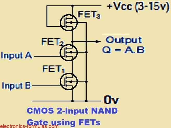
In this example of a basic CMOS gate we see that the circuit consists of three N-channel enhancement-mode MOSFETs (Metal-Oxide-Semiconductor Field-Effect Transistors). Here, two of the MOSFETs which are indicated as FET1 and FET2, are hooked up with each of the inputs while the third MOSFET, FET3, works like a switching device and is permanently biased to remain “ON” via its gate connection.
When either or both inputs indicated as “A” and “B,” are supplied with a logic level “0” meaning if they are grounded, the corresponding MOSFETs, FET1 or FET2, turn “OFF.” When this happens it causes the FET3 to generate a logic “1” (HIGH) output from its source terminal, because we don’t have any current flowing through FET1 or FET2 to influence the state of FET3.
On the other hand suppose if we supply both the inputs “A” and “B” with a logic level “1” (HIGH) voltage, then current flows through both FET1 and FET2 causing them to switch “ON.” As a result the output state at Q becomes a logic level “0” because both FET1 and FET2 are conducting and thereby creating a low output condition at the source of FET3. This behavior is similar to that of a NAND gate, in which all inputs must be “1” for the output to be “0.”
As we see more advancements in circuit design, mainly for the switching speed, low power usage, and reduced signal delays, these have paved the way for the development of the standard CMOS 4000 “CD” family of logic ICs. These logic families are designed to work hand in hand with the TTL (Transistor-Transistor Logic) IC counterparts.
Just like TTL logic gates, the CMOS 4000 series also contains all the major types of digital logic gates and devices. To illustrate we can take the example of the IC CD4011 which is a quad 2-input NAND gate, and the IC CD4001 which is a quad 2-input NOR gate. You can get these ICs along with their various sub-families.
The CMOS (Complementary Metal-Oxide-Semiconductor) logic circuits, just like their TTL counterparts, make use of both N-channel and P-channel transistors on the same chip in order to execute the many different logic functions.
But, you may also find that CMOS ICs have some drawbacks compared to TTL ICs, for example, these tend to be more sensitive to static electricity and can be quickly damaged when subjected to static electricity. However, while the TTL logic gates are specifically designed to operate with a single +5V power supply, CMOS logic gates can function with a wide supply voltage ranging from +3V to +18V.
Standard Sub-families of CMOS ICs
4000B Series: Standard CMOS
This was one of the first generations of CMOS logic gates which were first introduced in the early 1970s.
These ICs are designed to operate with a voltage range between 3.0V to 18V DC, and are popular for their original buffered CMOS technology which provides stable and reliable performance over a wide range of voltages.
74C Series: 5V CMOS
The 74C series of ICs are designed to be compatible with standard 5V TTL (Transistor-Transistor Logic) devices, which means that we can use these ICs interchangeably with TTL ICs in any of our desired applications.
Although these ICs use CMOS technology for their internal logic switching you will find that their input characteristics are designed to work similarly like those of TTL logic, so that we can easily interface them with TTL-based systems. These can also operate over a wide voltage range from 3.0V to 18V DC.
But please be aware that CMOS logic gates and components are sensitive to static electricity, and to prevent it from getting damaged, you must always follow proper precautions. Always make sure that you work on antistatic mats or grounded workbenches and wear an antistatic wristband, and only remove components from their antistatic packaging when you’re ready to use them.
In my next upcoming tutorial on Digital Logic Gates I will make you well versed with the function of the digital Logic AND Gate, and we will learn how it can be used to with both both TTL and CMOS logic circuits. I will be also discussing its Boolean Algebra representation and truth tables.
References: Logic gate