The Input Impedance ZIN, or what people call as the Input Resistance, is important thing when making transistor amplifier circuits. It helps us to tell what kind of amplifier it is by looking at input and output impedance and also power and current ratings.
Now amplifier impedance value is very important for circuit analysis, especially when joining many amplifier stages one after another.
Main goal is to stop signal from getting too much distortion when it passes through the circuit.
The input impedance of amplifier is what source “sees” when giving signal to amplifier. If too low, it can cause problems to previous stage and maybe change frequency response and output signal level.
But most of the time, common emitter and common collector amplifier circuits have high input impedance, so not a big problem.
Some amplifier designs like common collector amplifier circuit already have high input impedance and low output impedance just because of how they are built.
Amplifiers can have high input impedance low output impedance and any gain, but if input impedance is too low, then maybe we need to change output impedance of the previous stage. If not possible, then better to use buffer amplifier stage to fix the problem.
Now besides voltage amplification Av, an amplifier also needs to do current amplification Ai, and also need to give power amplification Ap.
And also an amplifier needs to have other things like high input impedance ZIN, low output impedance ZOUT and also some bandwidth Bw. In best case, the perfect amplifier will have an unlimited or infinite input impedance and zero output impedance, but this may be only in a theory.
Understanding Input and Output Impedance

Ok, so in many ways we can think of an amplifier like a kind of “black box” with two input terminals and two output terminals as shown.
This idea helps us use a simple h-parameter model of the transistor, then we can figure out the DC set point and operating parameters of the amplifier. But actually, one of these terminals is common for both input and output, which means it acts as ground or zero volts.
Now when we see from the outside, we find these terminals have something called input impedance ZIN and output impedance ZOUT.
Basically, the input and output impedance of an amplifier is just the ratio of voltage to current going in or out of these terminals.
The input impedance can change depending on the source supply feeding the amplifier and the output impedance can also change based on the load impedance RL connected across the output.
So, the signals getting amplified are usually AC signals and the amplifier circuit behaves like a load Z for the source.
The input impedance of an amplifier can be from just a few ohms (Ω) in some cases to a few thousand ohms (kΩ) for bipolar transistor circuits then up to millions of ohms (MΩ) when we use FET-based transistor circuits.
When we connect a signal source and a load to an amplifier the electrical behavior of the amplifier circuit can be interpreted as shown below.
Analyzing Output and Input Impedance Model

Ok let us break it down. We have a signal voltage VS and the internal resistance of the signal source RS.
Then there is the load resistance RL which is connected across the output.
Now we can expand on this idea by looking at how the amplifier connects to the source and load.
So when an amplifier is connected to a signal source, the source basically “sees” the input impedance Zin of the amplifier as a load.
But the input voltage Vin is what the amplifier sees across this input impedance Zin. Then we can model the amplifier’s input as a simple voltage divider circuit, like this.
Circuit Model showing Amplifier Input
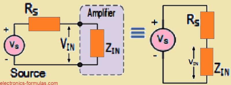
VIN = VS * (ZIN / (RS + ZIN))
Now here the same thing happens with the amplifier’s output impedance. When we connect a load resistor RL to the amplifier’s output, then the amplifier kind of turns into the source that powers the load.
So, now the output voltage and impedance just become the source voltage and source impedance for the load, as you can see below.
Circuit Model for the Amplifier Output
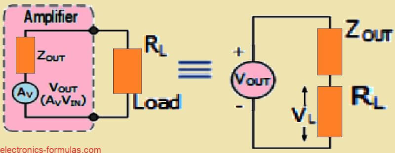
VL = VOUT * (RL / (ZOUT + RL))
So now we see that the input and output stuff of an amplifier, we can model both like a simple voltage divider network. The amplifier itself, we can connect in Common Emitter (emitter grounded), Common Collector (emitter follower), or Common Base setups.
But for now, in this article we will check out the bipolar transistor in a common emitter setup, like we saw before.
Common Emitter BJT Amplifier Circuit
So here Now let us talk about the so-called classic common emitter setup. It uses a potential divider network to bias the transistor’s Base. The power supply Vcc and those biasing resistors decide how the transistor operates making it work in the forward active mode.
Now, if there is no signal current going into the Base then no Collector current flows meaning the transistor stays in cut-off. So, the Collector voltage just stays the same as Vcc.
But, when a signal current goes into the Base it makes a current flow through the Collector resistor Rc. This creates a voltage drop across Rc, which then makes the Collector voltage go down.
Then here is the interesting part. The Collector voltage changes in the opposite direction compared to the Base voltage, so basically the polarity gets reversed.
That is why the common emitter setup gives a big voltage amplification and also keeps a steady DC voltage level. The output voltage is taken from the Collector and we use resistor RL as the load across this output as shown.
BJT Common Emitter Amplifier with Single Stage
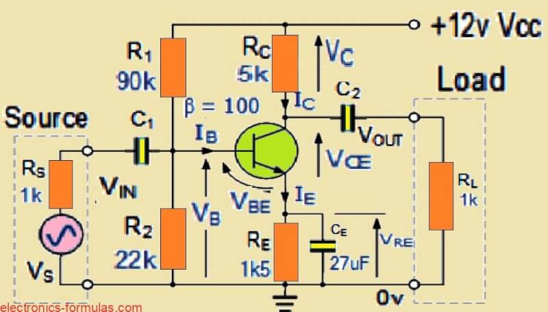
Now we can calculate the values of the resistors needed for the transistor to work in the middle of its linear active region which is called the quiescent point or Q point, but let us do a quick review so we understand better how the amplifier’s values were found and then we can use this circuit to find the input impedance of the amplifier.
Here let us start by making a few simple assumptions about the single-stage common emitter amplifier circuit above to define the operating point of the transistor.
We assume that the voltage drop across the Emitter resistor VRE is 1.5V, the quiescent current IQ is 1mA, then the current gain (Beta) of the NPN transistor is 100 (β = 100) and the corner or breakpoint frequency of the amplifier is given as: ƒ-3dB = 40Hz.
Then since the quiescent current with no input signal flows through the Collector and Emitter of the transistor, we can assume that: IC = IE = IQ = 1mA. So now we can use Ohm’s Law…
RE = VRE / IE
= 1.5V / 1mA
= 1500Ω or 1.5kΩ
When we turn the transistor completely ON, meaning when it is in full saturation mode then the voltage drop across the collector resistor Rc is going to be about half of Vcc minus VRE.
But this configuration is important because it allows the output signal to swing as much as possible from peak to peak. So the signal can operate right in the middle without running into any kind of clipping issues that might distort it.
VRC = (VCC – VRE) / 2
= (12V – 1.5V) / 2
≈ 5V
RC = VRC / IC
= 5V / 1mA
= 5kΩ
It is important to take into consideration that the direct current voltage gain of the amplifier, when there is no input signal present can be determined by utilizing the formula –RC/RE.
Furthermore it should also be observed that the value of the voltage gain is negative in nature. This is due to the reason that the output signal undergoes an inversion, meaning that it becomes phase shifted by 180 degrees in relation to the initial input signal.
Since the NPN transistor is in a forward biased condition, the Base Emitter junction effectively functions in a manner similar to that of a diode that is forward biased.
As a consequence of this characteristic, the voltage present at the Base terminal will be higher by approximately 0.7 volts in comparison to the voltage that is present at the Emitter terminal.
This can be mathematically expressed as Ve + 0.7V. Hence the potential difference that exists across the Base resistor denoted as R2 will be equal to:
VR2 = VRE + VBE
= 1.5V + 0.7V
= 2.2V
We may also determine the Base voltage Vb across R2 using the usual voltage divider calculation provided the two biasing resistors are readily available.
VR2 = VCC * (R2 / (R1 + R2))
According to the provided information, the quiescent current is 1 mA. As a result a collector current of 1 mA over the 12 volt supply Vcc biases the transistor. The collector current Ic = β * Ib varies in proportion to the base current.
Base current entering the transistor is going to be as shown below if the transistor’s DC current gain Beta (β) is set to 100:
β = 100 = IC / IB
IB = IC / β
= 1mA / 100
= 10µA
The DC bias setup is made using a voltage divider with two resistors R1 and R2. This setup decides the DC working point of the circuit. Earlier we figured out that the Base voltage should be 2.2 volts. So we have to pick the right proportion of R1 and R2 to get this voltage from the 12V supply Vcc.
Normally in a common emitter amplifier circuit using a voltage divider for DC biasing, the current passing through R2 (the lower resistor) is chosen to be ten times more than the DC Base current. This helps in keeping the bias stable. To find the correct value of R2 we use the formula:
IR2 = 10 * IB
= 10 * 10µA
= 100µA
R2 = VR2 / IR2
= 2.2V / 100µA
= 22kΩ
The voltage that appears across resistor R1 is simply the supply voltage minus the Base bias voltage. That means R1 has to drop the remaining voltage after the Base gets its required 2.2V from the 12V supply.
Also since resistor R2 is designed to carry a current that is 10 times the Base current, so the upper resistor R1 must handle both this current and the transistor’s actual Base current (Ib).
This means that the total current flowing through R1 is the sum of these two which equals 11 times the Base current. This is how the current distribution works in the voltage divider network.
VR1 = VCC – VB
= 12V – 2.2V
= 9.8V
IR1 = IR2 + IB
= 100µA + 10µA
= 110µA
R1 = VR1 / IR1
= 9.8V / 110µA
= 90kΩ
In a common emitter amplifier, the reactance Xc of the Emitter bypass capacitor is normally picked to be one-tenth (1/10th) of the Emitter resistor RE’s value when the frequency reaches the cut-off point.
The amplifier specs say the -3dB cutoff frequency is 40Hz. So we can find out the value of the bypass capacitor CE using this information with the formula:
At 40Hz, XC = (1 / 10) * RE
= 1500 / 10
= 150Ω
CE = 1 / (2π f XC)
= 1 / (2π * 40 * 150)
= 27µF
Now that we have fixed values for our simple emitter amplifier so we can calculate its input and output impedance and find values for coupling capacitors C1 and C2.
Fundamental BJT Emitter Amplifier Circuit Model
The general formula for input impedance of any circuit is ZIN = VIN/IIN. The DC bias circuit decides the DC working “Q” point of the transistor. The input capacitor C1 works like an open circuit stopping any outside DC voltage from passing through.
At DC (0Hz), the input impedance (ZIN) is very high. But when an AC signal enters, things change because capacitors act like short circuits at high frequencies and let AC signals pass.
The formula for AC input impedance at the Base is:
ZIN = REQ || β(RE + re)
Here, REQ is the total resistance to ground (0V) from the Base bias network, and re is the internal signal resistance inside the forward-biased Emitter.
If we treat the 12V power supply Vcc as a short circuit for AC signals (because Vcc acts like a short to AC), then we can recreate the common emitter bjt amplifier circuit like this:

When power supply is shorted, many resistors become in parallel with the transistor. If we look at only input side and think capacitor C1 is a short for AC, we can now redraw circuit to find input impedance as given below:
BJT Amplifier Circuit’s Input Impedance

Before, in the last Common Emitter Amplifier tutorial, we told that the inside signal resistance of the Emitter layer is same as 25mV ÷ Ie. This 25mV is the inside voltage drop, and IE is just equal to IQ. So, for the amplifier circuit shown above, the AC resistance value re of the Emitter diode comes out as:
Resistance of the BJT Emitter Pin to signals
re = 25mV / IE
= 25mV / 1mA
= 25Ω
In this formula, re stands for a tiny internal resistor that sits in series with the Emitter. Since Ic divided by Ib gives β, the transistor’s Base impedance will simply be β times re.
Now if the bypass capacitor CE is missing from the amplifier design then the impedance value turns into β times (RE + re), which makes the amplifier’s input impedance much higher.
But in our case, the bypass capacitor CE is present. So the input impedance ZIN of this Common Emitter amplifier is the actual impedance that the AC source feeding the amplifier will “see” and this is found using the formula:
Formula for Calculating the Input Impedance of a BJT Amplifier Circuit
ZIN = R1 || R2 || β(re)
1 / ZIN = 1 / R1 + 1 / R2 + 1 / β(re)
1 / ZIN = 1 / 90k + 1 / 22k + 1 / (100 × 25)
1 / ZIN = 1 / 90000 + 1 / 22000 + 1 / 2500
1 / ZIN = 0.00001111 + 0.00004545 + 0.0004
1 / ZIN = 0.00045656
ZIN = 2190Ω or 2.2kΩ
That 2.2 kiloohms, that is the input impedance. Think of it as the resistance the amplifier presents to any incoming signal. If we also know the signal source’s resistance which is 1 kiloohm in our simple example, we can add that to the amplifier’s input impedance (ZIN) if we need to.
But what if we took out that bypass capacitor CE from our circuit? What would happen to the amplifier’s input impedance?
The general equation for calculating impedance stays the same, but now we have to include the emitter resistor, RE, in the β(RE + re) part of the formula.
That’s because, without the bypass capacitor RE isn’t shorted out at higher frequencies anymore. So the input impedance of the amplifier without CE will be found using this adjusted calculation:
Calculating the BJT Amplifier Circuit’s Input Impedance without Bypass Capacitor
ZIN = R1 || R2 || β(RE + re)
1 / ZIN = 1 / R1 + 1 / R2 + 1 / β(RE + re)
= 1 / 90k + 1 / 22k + 1 / (100 × (1500 + 25))
= 1 / 90000 + 1 / 22000 + 1 / 152500
= 0.00001111 + 0.00004545 + 0.00000656
1 / ZIN = 0.00006312
ZIN = 15842Ω or 15.8kΩ
Here we can clearly see that when we put this capacitor across the Emitter leg, it completely changes how the circuit behaves in terms of input impedance.
Then what happens is, without this capacitor, the impedance is quite high at 15.8kΩ but as soon as we connect it, then impedance drops hugely to just 2.2kΩ in our given example. So now we understand that this small capacitor makes a big impact.
But that’s not all! Later we will also see that by adding this bypass capacitor which we call CE we can actually boost the gain of the amplifier.
Now when we were calculating the input impedance for this amplifier circuit, we assumed that all capacitors in the circuit act as if they have zero impedance (Xc = 0) when AC signals pass through them but for DC currents, they behave as if they have infinite impedance (Xc = ∞). So that was our basic assumption while doing our math.
Now that we already know that the input impedance of this circuit, after bypassing, has come down to 2.2kΩ we can use this value to figure out the exact value of the input coupling capacitor which is labeled as C1.
This capacitor needs to be calculated so that it works correctly at the specific cut-off frequency we mentioned earlier which was given as 40Hz. So let’s go ahead and do that calculation now.
Formula for Calculating the Input Coupling Capacitor in a BJT Amplifier Circuit
C1 = 1 / (2π f3dB ZIN)
= 1 / (2π × 40Hz × 2.2kΩ)
= 1.8µF
We have previously determined the input impedance value for the circuit above for our single-stage common emitter amplifier, correct?
Thus, we can now attempt to determine this amplifier’s output impedance using the same kind of technique.
Amplifier Output Impedance

The impedance, or resistance, that the load will perceive when it looks back into the amplifier circuit when the input is zero is what we mean when we refer to an amplifier’s output impedance. Thus we can obtain a generic formula for output impedance in the same way as we did for input impedance earlier:
ZOUT = VCE / IC
However because these two resistors are connected in series across the supply voltage Vcc, the signal current that passes through the collector resistor RC also passes through the load resistor RL.
But if we only consider the transistor amplifier’s output and suppose that the output coupling capacitor C2 is functioning as a short circuit for AC signals, we may redraw the circuit in a fashion that assists us in accurately defining the amplifier’s output impedance, such as this:
BJT Amplifier Circuit’s Output Impedance
ZOUT = RC || RL
= 1 / RC + 1 / RL
= 1 / 5k + 1 / 1k
= 0.0002 + 0.001
1 / ZOUT = 0.0012
ZOUT = 833Ω
As we can see, the output impedance of the amplifier is the same as RC when connected in parallel with RL.
Output Impedance Equation
Zout = Rc || RL
1 / Zout = 1 / Rc + 1 / RL
1 / Zout = 1 / 5k + 1 / 1k = 0.0012
∴ Zout = 833Ω
The 833Ω number indicates that the load resistor RL has a direct connection across the transistor. But what happens if we eliminate RL completely? The amplifier’s output impedance will now be equal to the collector resistor RC nothing else, okay?
So now that we have the output impedance value for our amplifier circuit above, what do we do next? Now we may calculate the value of the output coupling capacitor C2 like we did previously, but this time at the 40Hz cut-off frequency, right?
Formula for Calculating the Output Coupling Capacitor
C2 = 1 / (2π f3dB ZOUT)
= 1 / (2π × 40Hz × 833Ω)
= 4.7µF
So again, here we can find the value of the coupling capacitor C2 in two different ways, one way is by including the load resistor RL and the other way is by not including it, ok?
Common Emitter Voltage Gain
Now when we talk about voltage gain for a common emitter circuit, we can calculate it using this simple formula:
Av = ROUT / REMITTER
Here ROUT is the output impedance we see in the collector side, and REMITTER is the equivalent resistance in the emitter side. But this emitter resistance can be different depending on whether the bypass capacitor CE is connected or not, ok?
If there is no bypass capacitor CE then we take RE + re where RE is the external emitter resistor, and re is the small internal resistance of the transistor itself.
Av = ROUT / (RE + re)
= 833Ω / (1.5kΩ + 25Ω)
= 833Ω / 1525Ω
= 0.546
But if the bypass capacitor is present then the calculation changes because the capacitor effectively shorts the AC signal, making REMITTER much smaller.
Av = ROUT / re
= 833Ω / 25Ω
= 33.3
Ok, so now here we can clearly see that when we add the bypass capacitor into our amplifier design, it makes a huge difference in the voltage gain Av right? The gain jumps massively from just 0.5 all the way up to 33! That is a big change, ok?
But now, one important thing to note is that the common emitter amplifier’s gain does not become infinite when the external emitter resistor is completely bypassed by the capacitor at high frequencies, ok? Instead the gain settles at a finite value given by this formula:
Av = ROUT / re
Now another thing we saw is that as the gain goes higher, the input impedance of the amplifier actually goes lower. Without the bypass capacitor, the input impedance was 15.8kΩ but after adding the capacitor it dropped way down to just 2.2kΩ, correct?
So it means that increasing the voltage gain can be a good thing in most amplifier circuits but there is a trade-off, our input impedance becomes smaller which might not always be good thing.
Conclusions
So in this tutorial we saw how we can find the input impedance of a common emitter amplifier. What we do is, we first short out the supply voltage then we take the voltage divider bias circuit and just treat it like two resistors in parallel.
Now when we look into this divider network, we see an impedance (R1 || R2) but this impedance is usually much smaller than the impedance we get when we look straight into the transistor’s Base which is β(RE + re). Why? Because, as the AC input signal varies, it changes the Base bias of the transistor and that in turn controls how much current flows through the transistor.
Now, there are many ways to bias a transistor, ok? That means we can have different single transistor amplifier circuits, each having their own different input impedance equations and values.
But if we want the total input impedance of the whole amplifier stage along with the source impedance, then we must also consider Rs. In that case, the total input impedance becomes (Rs + R1 || R2).
Next if we talk about output impedance, for a common emitter stage, it is simple. It is just the collector resistor in parallel with the load resistor (RC || RL) but if there is no load connected, then it is just RC. The voltage gain Av of the amplifier depends on the ratio RC/RE.
Now, if we add an emitter bypass capacitor CE then it creates an AC path to ground for the Emitter. What does this do? It shorts out the emitter resistor, RE at high frequencies. So now in the Emitter leg circuit, only the small-signal emitter resistance re is left.
What happens because of this? The voltage gain of the amplifier increases as frequency increases. For example the gain might go from 0.5 up to 33. But this also has a side effect. The input impedance of the amplifier decreases, for example, it might drop from 18.5kΩ down to 2.2kΩ.
Now if we remove this bypass capacitor, then opposite happens. The voltage gain Av decreases, but the input impedance ZIN increases. So how do we balance this?
One way is to add a resistor in series with CE. This creates something called a “split-emitter” amplifier circuit. It is kind of a middle ground between a fully bypassed and a completely unbypassed amplifier.
But remember, adding or removing this bypass capacitor does not change the amplifier’s output impedance.
So, what do we learn from all this? The input and output impedances of an amplifier are very important because they help define how the amplifier transfers signals. They control the relationship between the output current Ic and the input current Ib. And if we know the input impedance of an amplifier, we can use it to draw the output characteristic curves of the amplifier.
References:
What is the actual input resistance of a BJT transistor (amplifier circuit especially)?
Leave a Reply