We already saw in our earlier tutorial on FET amplifiers that we can make simple one-stage amplifiers using JFETs or junction field effect transistors, right? But then we have other types of field effect transistors too and these can also be used to build an amplifier. So now, in this tutorial we will look at another type, which is the MOSFET amplifier.
Now MOSFET stands for Metal Oxide Semiconductor Field Effect Transistor. This is a really good choice when we want to make small-signal linear amplifiers.
Why? Because its input impedance is extremely high so it is very easy to bias.
But if we want a MOSFET to give proper linear amplification then we must run it in its saturation region. This is different from a Bipolar Junction Transistor (BJT) which works in a different way. But still just like the BJT, we must bias the MOSFET around a fixed Q-point in the middle.
Now MOSFETs allow electric current to pass through a conducting area which we call “the channel.” So if we apply a correct gate voltage then we can make this conducting channel wider or narrower. This means we are controlling how much current flows through it.
So what happens here is that when we apply a gate voltage then it creates an electric field around the gate terminal. This electric field affects how the channel conducts electricity. That is why we call it a field-effect transistor!
In simple words we can control how the MOSFET works by forming or “enhancing” its conductive channel between the source and drain terminals. This type of MOSFET is called an n-channel Enhancement-mode MOSFET.
Now what this means is, if we do not give it a positive bias on the gate (or negative for p-channel), then no current will flow through the channel. No bias, no conduction, simple as that.
But here is something important—you will see that different MOSFETs have different characteristics. So we cannot just apply the same biasing to all of them.
Each MOSFET needs its own biasing method. Just like how a common emitter amplifier using a bipolar transistor needs proper quiescent biasing, a common source MOSFET amplifier also needs to be biased properly at a suitable quiescent value.
But before we go into all that, let us first refresh our memory on the basic characteristics and working of a MOSFET, ok?
Understanding Enhancement N-channel MOSFET
Now let us talk about Enhancement N-channel MOSFET right? So first we have to understand how this MOSFET thing is different from a Bipolar Junction Transistor or BJT in short.
So what is the basic difference? We look at the terminals first. A BJT has three terminals and we call them Collector, Emitter and Base.
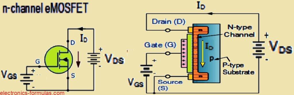
But if we see a MOSFET then we do not call them that. We give them different names. Here the three terminals are called Drain, Source and Gate, ok? So that is one big difference.
Now another important difference is how the gate is connected. In a BJT we see that the Base and Emitter are kind of directly connected because there is a PN junction there, ok? But in a MOSFET this Gate terminal is different. It is not directly connected to the channel at all.
Instead it has something called a metal gate electrode and this thing is fully insulated from the conductive channel. That is why we sometimes call it an Insulated Gate Field Effect Transistor or IGFET.
So in short in a MOSFET the Gate is kind of floating with an insulating layer in between not like a BJT where the Base-Emitter junction is physically touching.
Now let us talk about our Enhancement N-channel MOSFET (NMOS). In this one if we check the main semiconductor material then we see that the bulk substrate is made of p-type material.
That means the basic body of the transistor is p-type. But the Source and Drain these two are made of n-type material.
That is how it is built. Then what happens? We apply a supply voltage to this MOSFET and this voltage is positive.
When we apply a positive voltage to the Gate terminal then what happens?
The positive Gate voltage starts pulling electrons towards itself from the p-type substrate right under the Gate area.
Now here what is happening is very important.
Because of this extra gathering of electrons under the Gate suddenly we see that this p-type region under the Gate starts behaving like n-type. It is like magic!
The p-type substrate which originally had holes now gets filled with free electrons and that creates a conductive path or channel between Source and Drain.
And that is how current starts flowing through the channel.
Now if we flip this and take a p-channel MOSFET (PMOS) then the whole thing happens in the opposite way.
Here we apply a negative voltage to the Gate.
What does this do? It pulls holes (which are positive charge carriers) under the Gate region because now the negative Gate attracts them.
These holes gather and form a conductive channel in the n-type substrate and the p-type channel appears which allows current to flow.
So in our n-channel MOS transistor we see something very clear. If we increase the positive voltage at the Gate then more and more electrons keep gathering near the Gate region.
As a result the conductive channel keeps getting wider and wider and this allows more current to flow from the Drain to the Source.
Because of this behavior where we keep increasing the Gate voltage and the channel keeps getting enhanced we call it an “Enhancement MOSFET.” That is why this name exists!
How Enhancement MOSFET Amplifier Works
Now we are talking about this thing called an Enhancement MOSFET, or eMOSFET, right? So first we have to understand that this thing is a normally-off device, meaning when we do not apply any gate-to-source voltage then it does not conduct at all. It just stays off.
That is why we call it normally-off.
But there is another type of MOSFET called the Depletion MOSFET, and that one is different.
It is normally-on.
That means even when the gate voltage is zero, then it still conducts unlike our eMOSFET which stays off in that condition.
Now why does this happen? It is because of the way an enhancement MOSFET is built and how it works.
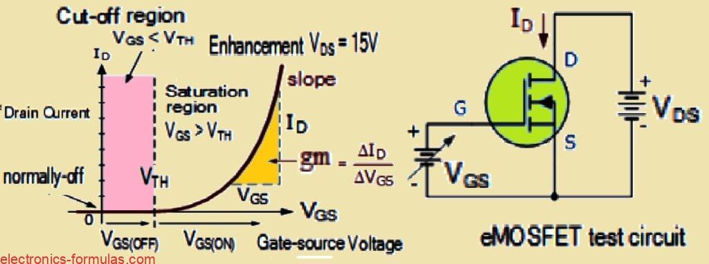
So for this type of MOSFET, there is something called a threshold voltage VTH. This is the minimum voltage we must apply between the gate and source before the MOSFET even starts conducting.
If the gate-source voltage VGS is less than this threshold voltage then no current flows. The MOSFET just stays off.
But once we keep increasing the gate voltage above this threshold then something happens. The MOSFET starts conducting, and the current through the drain which we call drain current ID (or sometimes IDS for drain-source current) also starts increasing.
This is kind of similar to what happens in a bipolar transistor where more base voltage increases collector current. Because of this behavior, this enhancement MOSFET becomes very useful for making MOSFET amplifier circuits.
Now we can think about the conductive channel inside the MOSFET like a variable resistor that we can control using the gate.
The more voltage we put at the gate, the more we change this resistance and control how much drain current passes through the n-channel. So how do we study this behavior?
One way is to make a graph. We take measurements and plot a transfer characteristics graph that shows the i-v relationship between drain current and gate voltage.
This graph helps us to understand how the MOSFET responds when we apply different gate voltages.
I-V Characteristics of an N-channel eMOSFET
Now let us take a case where we have a fixed drain-source voltage, VDS, applied across our eMOSFET, right?
So when we do this then we can start changing the gate-source voltage VGS and at the same time we note down how much drain current ID is flowing.
Then we keep doing this for different values of VGS and make a graph. This graph tells us about the MOSFET’s forward DC characteristics.
Now these characteristics are very important because from here we can get something called transconductance, gm, which is a key parameter of the MOSFET.
Now what is this transconductance? It is basically how much the output drain current changes when we change the input gate voltage.
That is why we say it represents the gain of the transistor. If we look at the transconductance curve on the graph then we can see its slope at any point.
This slope is what gives us the transconductance value. We define it as gm = ID / VGS, but only when VDS is kept constant.
So let us take an example now. Suppose we have a MOS transistor and we see that when VGS is 4V then the drain current ID is 3mA.
But now if we increase VGS to 8V then what happens? We check again and now the drain current is 16mA. Therefore:
gm = ΔID / ΔVGS = (16 – 3) × 10^-3 / (8 – 4) = 3.25mS
Now this ratio that we just talked about, this gm, we call it the static or DC transconductance of the transistor, ok? It is actually a short form for “transfer conductance.”
This thing tells us how much current changes when we change the voltage and we measure it in Siemens, S. One Siemens is the same as saying one amp per volt.
So now why is this important? It is because when we build a MOSFET amplifier circuit then the voltage gain of this amplifier depends on two things. One is the transconductance gm and the other is the value of the drain resistor.
So both of these decide how much gain we are going to get from the MOSFET amplifier.
Now let us take a special case, ok? Suppose we make VGS equal to 0V then what happens? Now because there is no voltage applied to the gate then no electric field is created around the gate region.
That means this electric field is not strong enough to form or activate the n-type channel inside the MOSFET. So now no current flows through the drain-source channel.
The MOSFET just does nothing. It is fully switched off. That is why we say that in this condition, the MOSFET is in its “cut-off” region. It behaves just like an open switch, not allowing any current to flow.
So in simple words if we do not apply any gate voltage then this n-channel eMOSFET is just normally off. It will not work. This is why in the eMOSFET circuit symbol we always show the channel as a broken line because it starts off disconnected.
But if we look at a depletion-mode MOSFET then we will see that it has a continuous channel line in its symbol.
That is because depletion-mode types are normally on which means they start conducting even when there is no gate voltage.
Now what happens when we slowly, step by step, keep increasing this positive gate-source voltage VGS? So as we do this then the field effect inside the MOSFET starts getting stronger.
That means the conductivity of the channel regions begins to improve little by little. Then at one particular voltage level, the channel suddenly starts conducting.
This special voltage level is what we call the threshold voltage VTH right?
Now if we keep increasing VGS even more then the conductive channel inside the MOSFET keeps getting wider and better which means the resistance of this channel keeps decreasing. Now because of this the drain current ID starts increasing more and more.
But here is something very important. The gate of this MOSFET is electrically isolated from the channel.
That means the gate itself does not allow any current to flow through it. It just controls the channel like a switch but does not conduct anything. Because of this, a MOSFET amplifier has a very, very high input impedance.
It means that our n-channel enhancement MOSFET stays fully switched off when the gate-source voltage VGS is lower than this threshold voltage VTH.
But the moment we make VGS higher than VTH then the channel starts conducting and the MOSFET enters saturation mode.
Now when our eMOS transistor is working in this saturation region then the drain current ID is decided by this formula:
Calculating Drain Current of eMOSFET
ID = k(VDS – VTH)2
Now one thing we must remember. The values of k which is the conduction parameter, and VTH which is the threshold voltage are not the same for all eMOSFETs. These values are different for different MOSFETs. And we cannot change them physically.
Why?
Because these values depend on certain fixed things like the material used inside the MOSFET and the shape and size of the device which are all decided when the transistor is manufactured.
So once it is made, these values stay fixed and we just have to work with whatever the manufacturer has given.
Now let us talk about this static transfer characteristics curve. When we look at this curve on the right, we can see that its shape is usually like a parabola at first which we also call the square law region. Then after this the curve moves into a straight-line section.
What does this curve tell us? It tells us how much the drain current ID increases when we increase the gate-source voltage VGS. This increase in ID for a given increase in VGS is what decides the slope or gradient of this curve when we keep the drain-source voltage, VDS, fixed.
Now here is something very important we must understand, ok? When we turn on an enhancement MOS transistor, it does not suddenly switch on like a simple mechanical switch. No, it turns on gradually, step by step.
So if we want to use a MOSFET properly as an amplifier then we must make sure to bias its gate terminal at a voltage level that is higher than its threshold voltage, VTH. Otherwise, it will not amplify properly.
Now how do we do this gate biasing? We can do this in many different ways. For example we can use two separate voltage supplies or we can use drain feedback biasing or we can use zener diode biasing and so on. There are many techniques but no matter which one we use one thing is always important.
We must make sure that the gate voltage is always higher than the source voltage by at least more than VTH.
Now in this tutorial about MOSFET amplifiers, we are going to use one of the most famous and widely used biasing methods. It is called the universal voltage divider biasing circuit.
This method is very popular because it provides a stable gate voltage without depending on external power supplies.
How to do DC Biasing of MOSFET
Now let us talk about this universal voltage divider biasing circuit.
So this circuit is actually a very famous and widely used method for setting up the correct DC operating conditions in both bipolar transistor amplifiers and MOSFET amplifiers.
That means we can use it for both types of transistors.
Now why do people like to use this voltage divider biasing network?
One big reason is that it lets us bias a MOSFET or a bipolar transistor using just a single DC power supply.
That means we do not need multiple power supplies, just one is enough.
But now here is one thing we must be careful about.
We must properly decide the correct gate biasing for the MOSFET amplifier.
If we do not do this correctly then the amplifier will not work properly.
Now let us talk about how a MOSFET works in different modes.
A MOSFET has three different regions in which it can operate.
The first one is called the Ohmic region, also known as the Triode region.
Then we have the Saturation region, which is also sometimes called the Linear region.
And then we have the Pinch-off point which is another important thing to know about.
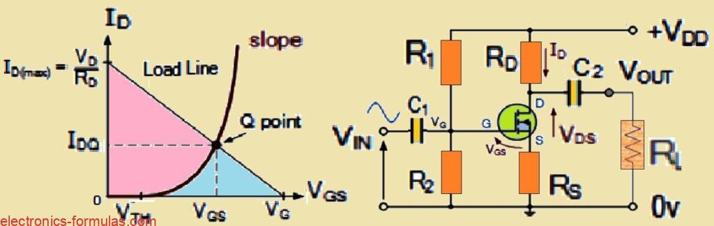
Now if we want our MOSFET to work as a proper linear amplifier then we must make sure to set up the right DC operating point.
This point is called the quiescent operating point or in short the Q-point.
This Q-point is very important because it decides how the MOSFET will behave when we apply an input signal.
Now for us to place this Q-point in the correct position, we must bias the MOSFET in such a way that it always operates inside its saturation region.
This is because only in this region, the MOSFET can work as a proper amplifier.
If we do not do this then the output signal may get distorted or may not amplify properly.
Now this Q-point is actually defined by the DC values of ID which is the drain current, and VGS, which is the gate-to-source voltage.
These values must be selected in such a way that the operating point sits right in the middle of the MOSFET’s output characteristics curve.
That means it must be positioned in such a way that there is enough room for the AC signal to move up and down without getting clipped or distorted.
Now as we already talked about before, the MOSFET enters the saturation region only when the gate-to-source voltage, VGS, becomes higher than the threshold voltage, VTH.
So now when we apply a small AC signal on top of this DC bias at the gate input, then the MOSFET will work like a proper linear amplifier.
This is exactly what we need to make sure our amplifier works as expected.
And if we set up everything correctly we can get a clean amplified output signal, just like how it is shown in the diagram.
What is eMOSFET DC Bias Point
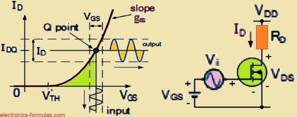
So here we see a common-source NMOS circuit, right? Now this input AC voltage Vi, we put this in series with a DC voltage. That DC voltage at the gate we fix that using the bias circuit. So total voltage from gate to source, we now get that by adding VGS and Vi.
Now this DC voltage at the gate, the power supply voltage VDD and the load resistor RD, these three things together decide the DC working condition which we call the Q-point.
But we must make sure this MOSFET works in the saturation zone, right? Thats important because only then we get the correct drain current which fixes the Q-point. Now when VGS increases then our bias point moves up on the graph. So drain current increases but VDS reduces.
Then when VGS reduces (like in the negative half of the input sine wave),bias point moves down. Now what happens? Drain current reduces but VDS increases.
Now if we want big voltage swing at the output we must bias this MOSFET well above its threshold voltage, right? That way it stays in saturation all the time, during the full AC cycle. But wait, we cannot increase the gate bias or drain current too much. There is a limit. So best way? We fix the Q-point somewhere around half of VDD and threshold voltage VTH.
For example let us say we build an NMOS common-source amplifier. The eMOSFET has a threshold voltage VTH of 2.6V, and our power supply is 14V, right? Then the DC bias point we calculate like this: 14V – 2.6V = 11.4V. But for easy working, we round that to 6V. Simple.
The ID – VDS Characteristics of MOSFETs
So like we said before, we can draw a graph to show how a MOSFET works when we keep the supply voltage VDD fixed but change the gate voltage VG.
But wait, if we really want to understand how an n-type enhancement MOSFET works inside an amplifier circuit then we must also see how the output behaves for different values of both VDD and VGS.
Now just like an NPN Bipolar Junction Transistor (BJT) we can make a set of output curves for this MOSFET. These curves show how the drain current ID changes when we keep increasing VG in an n-channel enhancement MOSFET. The graph shows that clearly.
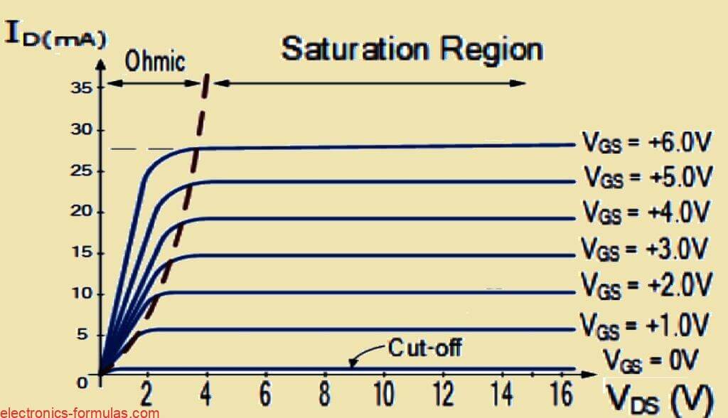
Now remember if we use a p-channel eMOSFET instead, we get a similar set of drain current curves. But here’s the thing—the gate voltage will have opposite polarity.
Basic Common Source MOSFET Amplifier
Before we talked about how to set the right DC conditions to bias an n-type eMOSFET, right? Now, if we add a small AC signal at the input then this MOSFET circuit can work like a linear amplifier.
But for that to happen, the Q-point must sit near the center of the saturation region. Also the input signal must be small enough so the output stays linear without distortion.
Check the basic MOSFET amplifier circuit shown below.
Analyzing a Basic MOSFET Amplifier circuit
So this is just a super simple common-source MOSFET amplifier. We got only one power supply here, that too only at the drain side, nothing else. Now for setting up the required gate voltage VG, we are just using a simple resistor divider. But for a MOSFET, we know that no current is going to enter its gate terminal. That means we can take this as a key thing and then assume a few basic points about how the DC stuff is working inside this amplifier?
Now let us write it down step by step:
VDD = ID * RD + VDS + ID * RS
= ID * (RD + RS) + VDS
So now from this we just rearrange a bit and get:
RD + RS = (VDD – VDS) / ID
Now from that, we can break it down further like this:
RD = (VDD – VD) / ID
RS = VS / ID
Now for the MOSFET, the gate-to-source voltage is just this simple:
VGS = VG – IS * RS
But for this MOSFET to actually work properly, we must make sure VGS is bigger than its threshold voltage VTH, right? And since we already know IS = ID in this case, then we can also say:
VGS = VG – ID * RS
So now if we solve this whole thing for VG, we get:
VG = VGS + ID * RS
Or simply, VG = VGS + VS
Ok, so now if we want to fix the MOSFET amplifier gate voltage at the exact level we need, then we have to pick the right resistor values for R1 and R2 in the voltage divider, right? And now, as we already said before, since no current is going inside the gate terminal of this MOSFET device, then we can simply write the voltage division formula like this:
VG = VDD(R2 / (R1 + R2))
Ok, so now it is very important to understand that this voltage divider equation is only setting the ratio between these two bias resistors R1 and R2, but not their exact values, right? That means we are just fixing how they relate to each other, not their actual resistor sizes. So it is always a good idea to select these resistor values as high as possible because then their I2 * R power loss will be lower and also the input resistance of this MOSFET amplifier will improve which is a good thing.
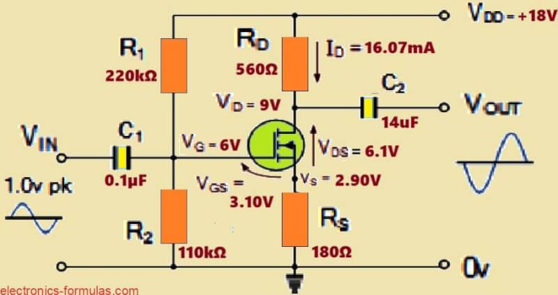
Solving a MOSFET Amplifier Problem #1
Ok, so now we want to build a simple common-source MOSFET amplifier. We are using an N-channel eMOSFET and this MOSFET has a conduction parameter of 45mA/V², and its threshold voltage is 2.5V.
Now the supply voltage we are working with is 18V. And for the drain resistor, we are picking 560Ω. Now, we want to set the drain voltage to 40% of VDD.
So with these new numbers, we have to find the correct resistor values for biasing the MOSFET properly. That means we need to calculate:
- How much current is flowing through the MOSFET
- What should be the source voltage (VS)
- What should be the gate voltage (VG)
- And finally what resistor values (R1 and R2) should we pick for the voltage divider at the gate.
- Once we get all that then we can draw the circuit again and see how it looks!
Step 1: Given Data
We are designing a common-source MOSFET amplifier with the following parameters:
- Supply Voltage (VDD) = 18V
- MOSFET Threshold Voltage (VTH) = 2.5V
- MOSFET Conduction Parameter (k) = 45mA/V²
- Drain Resistor (RD) = 560Ω
- Gate Bias Resistors:
- R1 = 220kΩ
- R2 = 110kΩ
Bias Condition:
The gate voltage (VG) should be one-third of VDD
VG = (1/3) * VDD
= (1/3) * 18V
= 6V
Step 2: Calculate the Drain Current (ID)
The MOSFET drain current ID is given by the quadratic equation:
ID = k * (VGS – VTH)^2
But first we will calculate VGS using the gate voltage equation:
VG = VGS + VS
Rearranging:
VGS = VG – VS
Since ID also determines VS (via RS) we proceed to solve both together.
Step 3: Express Source Voltage (VS) in Terms of ID
From Ohm’s Law, the source voltage is:
VS = ID * RS
Substituting into the VGS equation:
VGS = VG – (ID * RS)
Now substituting this VGS into the MOSFET current equation:
- ID = k * ((VG – ID * RS) – VTH)^2
- Expanding:
- ID = 45mA/V² * (3.5V – ID * RS)^2
This is a quadratic equation in terms of ID, so we now solve for RS to get a direct result.
Step 4: Solve for Source Resistor (RS)
ID = 45mA/V² * (3.5V – ID * RS)^2
Since we know ID also affects RS, let us assume a step-by-step approach to solve for ID.
Using Ohm’s Law on the drain resistor RD:
VD = VDD – (ID * RD)
For a symmetrical undistorted output, we bias the drain voltage VD to VDD/2:
- VD = VDD / 2
- = 18V / 2
- VD = 9V
- So:
- 9V = 18V – (ID * 560Ω)
- Rearrange for ID:
- ID = (18V – 9V) / 560Ω
- ID = 9V / 560Ω
- ID = 16.07mA
Now using VGS equation:
- VGS = VG – VS
- VGS = 6V – (ID * RS)
And from the MOSFET equation:
- ID = 45mA/V² * (VGS – 2.5V)^2
- Substituting ID = 16.07mA:
- 16.07mA = 45mA/V² * (VGS – 2.5V)^2
- (VGS – 2.5V)^2 = 16.07mA / 45mA/V²
- (VGS – 2.5V)^2 = 0.357
- VGS – 2.5V = √(0.357)
- VGS – 2.5V = 0.597V
- VGS = 3.10V
Now we solve for RS:
- RS = VS / ID
- And since:
- VS = VG – VGS = 6V – 3.10V = 2.90V
- RS = 2.90V / 16.07mA
- RS = 180.5Ω
- Rounding to a standard value:
- RS ≈ 180Ω
Step 5: Calculate Input Resistance (Rin)
The input resistance of the MOSFET amplifier is determined by:
Rin = (R1 * R2) / (R1 + R2)
Substituting values:
- Rin = (220kΩ * 110kΩ) / (220kΩ + 110kΩ)
- Rin = (24.2GΩ) / (330kΩ)
- Rin = 73.3kΩ
Step 6: Calculate Coupling Capacitors for 20Hz Cut-off
The high-pass filter equation is:
C = 1 / (2 * π * f * R)
(a) Input Coupling Capacitor (Cin)
- For input impedance Rin = 73.3kΩ, we calculate:
- Cin = 1 / (2 * π * 20Hz * 73.3kΩ)
- Cin = 1 / 9.2MΩ
- Cin ≈ 0.11µF
- Rounding to standard value:
- Cin ≈ 0.1µF
(b) Output Coupling Capacitor (Cout)
- For output impedance RD = 560Ω:
- Cout = 1 / (2 * π * 20Hz * 560Ω)
- Cout = 1 / 70.4kΩ
- Cout ≈ 2.26µF
- Rounding to standard value:
- Cout ≈ 2.2µF
Final Answer:
- Gate Bias Resistors:
- R1 = 220kΩ
- R2 = 110kΩ
- Input Resistance: Rin ≈ 73.3kΩ
- Drain Resistor: RD = 560Ω
- Source Resistor: RS ≈ 180Ω
- Drain Current: ID ≈ 16.07mA
- Gate-to-Source Voltage: VGS ≈ 3.10V
- Source Voltage: VS ≈ 2.90V
- Input Coupling Capacitor: Cin ≈ 0.1µF
- Output Coupling Capacitor: Cout ≈ 14µF
From the above calculated parts value we can now draw the finalized Single Stage MOSFET Amplifier circuit diagram as given below:
Conclusions
So now, when we use a MOSFET amplifier, or actually any kind of amplifier, the whole idea is to take a small input signal and make it bigger at the output, right? But we want the output signal to look exactly the same as the input, just amplified. This input signal can be either a current or a voltage but for a MOSFET to actually do the amplification job properly, we have to bias it in such a way that it keeps working inside its saturation region, ok?
Now if we talk about MOSFETs then we basically have two types of enhancement-mode MOSFETs. One is the n-channel type and the other one is the p-channel type. But here, in this MOSFET amplifier explanation, we are looking at the n-channel enhancement MOSFET which many people just call NMOS. This type of MOSFET works with positive gate and drain voltages compared to the source. But if we look at the p-channel MOSFET or PMOS then that one works the opposite way, meaning it needs negative gate and drain voltages compared to the source.
Now, when we talk about the saturation region of a MOSFET, the region where the drain current ID stays constant even if we change the drain-to-source voltage VDS. But for this to happen, we first need to bias the MOSFET properly so that it stays in this region, right? This happens when the MOSFET’s gate-to-source voltage VGS controls the drain current instead of the drain-to-source voltage. This is why we say the drain current is “saturated” in this region.
In an enhancement-mode MOSFET when we apply a voltage to the gate terminal, this creates an electrostatic field inside the MOSFET. This field increases the conductivity of the channel between the source and drain. This is totally different from what happens in a depletion-mode MOSFET, where the channel already exists and applying a gate voltage actually reduces its conductivity instead of increasing it.
Now this thing called the threshold voltage or VTH, is very important. It is the minimum gate voltage that we need to apply so that the MOSFET actually starts working. Below this voltage, the MOSFET just does not conduct properly, meaning no real amplification happens. But once we go above this threshold voltage then the drain current ID starts increasing. And this increase happens in proportion to (VGS – VTH)² when we are in the saturation region. This is exactly how a MOSFET is able to work as an amplifier, because this relation allows it to take a small input signal and turn it into a bigger output signal.
References:
Leave a Reply