
A NOT gate which is also known as an inverter, is a digital logic component with a single input and a single output. The basic function of a NOT gate is to invert the input signal to generate an exactly opposite signal at its output. For example, suppose if we apply input of a NOT gate with a logic high level (1), then its output will generate an opposite logic low level (0). Conversely if we supply the NOT gate input with a logic low level (0), then its output switches to a logic high level (1). We can explain this behavior through the Boolean expression as Ā = Q
In other words the NOT gate performs the logical operation of negation or inversion. You will find the NOT gate’s output Q is true (logic high) if and only if the input A is not true (logic low). Hence we can summarize the operational definition of the NOT gate as:
“If A is false, then Q is true.”
Logic NOT Gate using BJT
You can create a simple single input logic NOT gate by employing a RTL Resistor-transistor switch as illustrated below in which the input side can be seen directly connected with the transistors base. In order to obtain a perfectly inverted output at Q, it is important that the transistor is either fully-ON, or fully-OFF.


In digital circuits, we use Logic NOT gates to perform the logical NOT operation. We represent a standard NOT gate with a symbol that features a triangle pointing to the right with a small circle at its tip.
This small circle which we call an “inversion bubble,” signifies that the signal is being inverted or complemented. Also, you might see this inversion bubble not only in NOT gates but also in NAND and NOR gates where it indicates that the output is the result of applying the NOT function to the inputs. Depending on the design, the bubble can appear at either the input or output terminals or sometimes at both.
Symbol and Truth Table for Logic NOT Gate
Symbol


Truth Table
| A | Q |
| 0 | 1 |
| 1 | 0 |
Boolean Expression Q = not A or Ā, we can also read it as: inverse of A gives Q
While working with Logic NOT gates we know that they always generate an output signal which is the complement of their input signal. This is why they are called NOT gates. This basically means that when the input signal is “HIGH,” the output becomes the opposite of HIGH, meaning it will become “LOW.” But if the input signal is “LOW,” the output will not be “LOW” instead it will be “HIGH.” Since these NOT gates come with only a single input, we do not typically classify them as “decision” making devices, unlike AND or OR gates, which require two or more inputs.
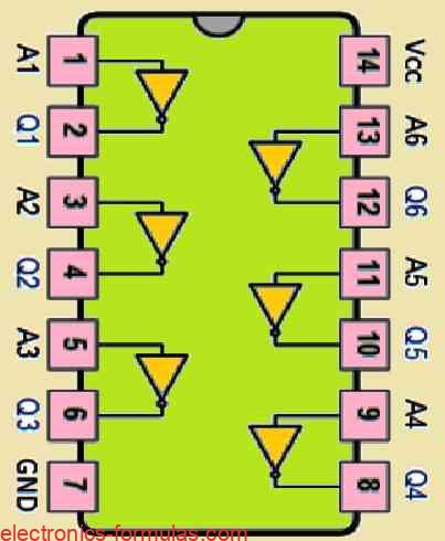
In a practical use you might find that NOT gate integrated circuits (ICs) mostly come with either 4 or 6 individual NOT gates inside a single package.
Inverting a Logic Signal using Active-low Input Bubble


When we draw a NOT gate we normally put a small circle, or “bubble,” at the end of the NOT gate, which indicates that the output signal from this gate will be inverted or complemented. Having said that, you may find that this bubble can also appear at the input of a gate to show that the input is active-LOW.
It is worth noting that this inversion is not just relevant to NOT gates only, rather it can be applied to any digital circuit or gate. The indication principle of the symbol remains the same, regardless of whether the bubble is at the input or output terminal of the gate. Basically we can imagine the bubble to be simply an indicator of an inverter function.
Equivalents of NOT gate using NAND and NOR Gates
We can easily replicate an Inverter or logic NOT gate using any standard NAND and NOR gates. This can be done simply by connecting ALL their inputs to a common input signal. The following example shows how this can be implemented.


You may also create a very simple logic inverter module by configuring just a single stage BJT circuit as shown below:


When we apply a high logic supply to base “A” of the the transistors, it switches ON, enabling the current to flow through its collector, causing a voltage drop to be generated across the resistor R, which also means that the BJT collector output point at “Q” will now sink to ground producing a zero voltage output at “Q“.
Conversely, if we now supply a low signal or 0V at the base input “A” of the BJT, it will be now switched “OFF” blocking the flow of current through the collector and the resistor, enabling an high output voltage to be generated at “Q” with a value almost equal to the +Vcc.
So in simple terms when a “HIGH” input voltage above 1V is applied to the base “A”, the collector output at “Q” turns LOW and when a “LOW” input supply voltage or a Ground voltage is applied at the base “A” causes the output voltage at “Q” to turn HIGH, producing the complement or inversion of the input signal.
Understanding Hex Schmitt Inverters
When we work with a standard Logic NOT Gate or inverter, we basically deal with a system which involves transistor switching circuits. These circuits tend not to switch from one state to the next instantaneously, instead you may find that there is always some delay in the switching action.
As we all aware that a transistors or BJTs work like a basic current amplifier, so it means BJTs can also operate in a linear mode. This also means that even a minute change of voltage in the BJT input can cause proportionate amounts of variations at its output, or simply the transistor would toggle between “ON” and “OFF” states in response any sort of noise or fluctuating signal in the circuit. Therefore just to makee sure the above issue is eliminated, we can use a concept called Schmitt Inverter or Hex Inverter.
From our earlier discussions, we understand that digital gates are designed to operate with just two logic voltage levels: Logic “1” and Logic “0”. For a TTL device, a logic “1” voltage input corresponds a level between 2.0V and 5V, whereas any voltage that is lower tan 0.8V may be regarded as Logic “0”.
A Schmitt Inverter is specifically designed to cope up with these voltage levels using an internal built-in hysteresis feature. When we apply an input signal which is higher than a specified “Upper Threshold Voltage” (UTV), it causes the output to turn LOW. This state is held constant until the input signal voltage drops below a specific “Lower Threshold Voltage” (LTV), at which point the output switches back to HIGH. So basically we find that a Schmitt Inverter incorporates the feature called hysteresis into its design to improve stability and reduce the impact of noise on its output response.


Due to the above explained switching characteristics of a Schmitt Inverter between an upper and lower threshold limits, we are able to achieve an “ON/OFF” switching output signal which is much cleaner and much faster, causing the Schmitt inverter to be very ideal for switching all types of slow-rising or slow-falling input signals. Hence, a Schmitt trigger allows the user to convert all types of analogue signals and voltages into digital signals as illustrated in the following diagram:
Schmitt NOT Gate Inverter


Because of their extreme versatility, Schmitt inverters are used to create oscillators or transform sine waves into square waves which are subsequently utilized as square wave clock signals.
Making an Efficient Digital Oscillator Circuit using Schmitt NOT Gate Inverter


In the first circuit above we see a simple low-power RC oscillator that generates a square wave output by use of a Schmitt inverter. Since the capacitor C is first entirely depleted, the inverter’s input is “LOW,” resulting in an output that is inverted from “HIGH.” The capacitor begins to charge as soon as we feed the inverter’s output back into its input and allow it to pass through resistor R.
As soon as the upper threshold voltage of the capacitor is reached, the inverter switches its state, turning the output to “LOW” and causing the capacitor to discharge through the resistor. After this, once the capacitor discharges to the lower threshold level, the inverter switches state again. Through this reverse-forward switching actions we are able to get an output with a square wave frequency, which characterizes a duty cycle of 33%, and we can calculate the frequency of this square wave output through the formula:
f = 680/RC
In the second circuit above, we are able to convert any sine wave input signal or simply any oscillating frequency, into a respective square wave output. To implement this we connect the input of the inverter with the junction of a potential divider network through which we are able to adjust and fix the quiescent point of the circuit. The purpose of the input capacitor is to filter out any potential DC component in the input signal so that only the sine wave signal can pass.
In the second circuit, when the input signal rises and crosses the upper threshold, it causes the output of the inverter to switch from “LOW” to “HIGH” which creates a positive pulse at the output that aligns with the rising edge of the input waveform.
Next when the input signal falls below the lower threshold, the output of the inverter gate switches from “HIGH” to “LOW” which triggers at the falling edge of the input waveform.
The above process of switching the output at each threshold produces a square wave output, which has an output pulse width corresponding to the period during which the input signal is between the upper and lower thresholds.
Now, if we connect a second Schmitt inverter to the output of the first inverter, the second inverter will receive the square wave output generated by the first inverter as its input.
The second inverter will again respond to the upper/lower transitions of the square wave, and as it processes the square wave output generated from the first inverter, the transitions that were previously producing output pulses on the positive rising edge will now result in output pulses on the negative falling edge of the original input signal, because the second inverter will also invert the square wave from the first inverter, effectively flipping the pulse timing from positive edges to negative edges.
So this shows that simply by adding a second inverter, we are able to control and alter the timing of the output pulses relative to the original input signal, allowing the circuit to generate output pulses on different edges of the input waveform.
The NOT gate inverter ICs that we are able to get easily from the market are given in the following table:
| Category | Part Number | Description |
|---|---|---|
| TTL Logic NOT Gates | 74LS04 | Hex Inverting NOT Gate |
| 74LS14 | Hex Schmitt Inverting Gate | |
| 74LS1004 | Hex Inverting Drivers | |
| CMOS Logic NOT Gates | CD4009 | Hex Inverting NOT Gate |
| CD4069 | Hex Inverting NOT Gate |
Pinout Diagram of a Popular IC 7404 Logic NOT Gate or Inverter

In our next lesson I will discuss the digital logic NAND Gate function applied for both TTL and CMOS logic circuits, and we will also learn the Boolean Algebra definition and truth tables for these logic gates.
References: Inverter (Logic Gate)