When we talk about distortion in an amplifier we are basically referring to how the output signal does not exactly match the original input signal it gets altered in some way.
One particular type of distortion that affects amplifiers with a push-pull design is something known as crossover distortion. This happens specifically at the point where the output waveform transitions through zero voltage also called the zero crossover point.
Now earlier we saw that one of the biggest downsides of using a Class A amplifier is that it is not very efficient when delivering full power. This is because it operates with a bias set around a central Q point which means it is always consuming a lot of power even when there is no signal.
However there is a way to significantly improve this efficiency almost doubling it. The trick is to modify the output stage of the amplifier and switch to a Class B push-pull configuration. That sounds fantastic from an efficiency standpoint but there is a small catch.
Most modern Class B amplifiers do not use transformers in their design anymore. Instead they are built with a complementary transistor pair at the output stage meaning they have two transistors working together to reproduce the signal.
Now here is where the real issue with push-pull designs comes in. These two transistors do not transition smoothly when handling both halves of the waveform.
Because of the way they are biased at zero cutoff there is a brief moment when neither transistor is conducting properly as the signal crosses zero volts.
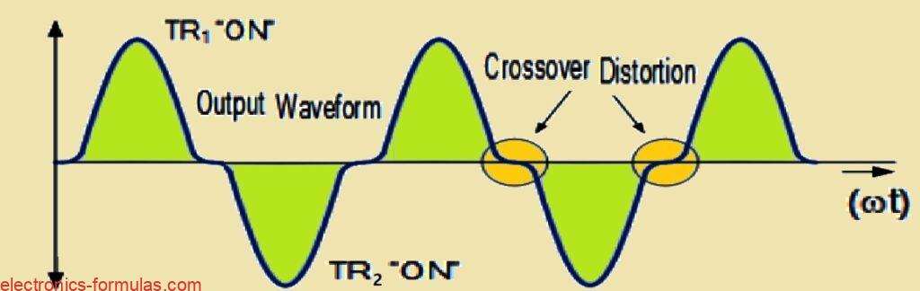
This results in a small but noticeable glitch in the waveform introducing a form of distortion. Since this distortion happens right at the point where the signal switches from one transistor to the other it is commonly known as crossover distortion.
Crossover Distortion: The “Flat Spot”
Imagine we are looking at a sound wave on a graph. Ideally it should be smooth and continuous. But when crossover distortion kicks in we see a little “flat spot” or a “deadband” right where the wave crosses the zero voltage line. It is like the wave stumbles a bit as it transitions from the positive to the negative side or vice versa.
Why Does This Happen? The Transistor Transition
The reason we get this flat spot is because of how transistors work in the amplifier. We know that transistors are like tiny switches that control the flow of electricity.
In an amplifier we have transistors that handle the positive and negative halves of the waveform. Ideally as one transistor turns “OFF” the other should turn “ON” at the exact same moment.
But here is the problem there is often a tiny delay. The transistor turning “OFF” might not happen instantly and the transistor turning “ON” might not start instantly either. So for a brief moment both transistors are actually “OFF” at the same time.
The Distorted Wave
When both transistors are “OFF” we get no output signal. This is what creates that “flat spot” or “deadband” at the crossover point. The output wave shape ends up looking a bit wonky and that is what we call crossover distortion, as shown below:
Okay let us try to explain this concept of distortion due to transistors not turning on immediately in a simple way keeping all the technical words and using “we” throughout.
The Ideal Instant On
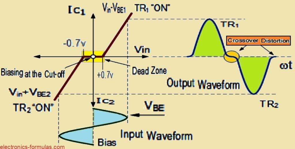
Now ideally to ensure that we do not get any distortion in the output waveform we would hope that each transistor starts conducting electricity the moment its base-to-emitter voltage creeps just above zero volts. This would give us a nice smooth transition.
The 0.7V Hurdle
But here is the thing we know this is not actually true. You see for silicon bipolar transistors the base-emitter voltage has to reach at least 0.7 volts before the transistor even begins to conduct any electricity.
This is because of something called the forward diode voltage drop of the base-emitter pn-junction. Think of it as a small energy barrier the voltage has to overcome.
The Flat Spot and Reduced Power
Because of this 0.7V requirement we end up with that “flat spot” we talked about earlier. This crossover distortion effect also has another downside it reduces the overall peak-to-peak value of the output waveform.
That means the maximum power output we can get from the amplifier is reduced as well. We are not getting the full swing of the wave.
Non-Linear Transfer Characteristics
We know that sometimes especially when the sound signals going into our amplifiers are small we can get something called crossover distortion.
It is not so bad when the signals are big because the input voltage is usually quite large anyway but when the input signals are small this distortion can really mess up the audio coming out of the amplifier.
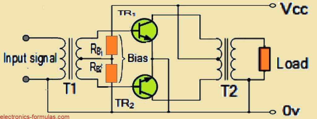
Now we have a clever trick to make this crossover distortion much less of a problem. It is called pre biasing. Basically we give the transistors a little nudge in the right direction by applying a small forward base bias voltage.
It is kind of like what we saw in the Transistor tutorial. We do this by using the center tap of the input transformer to send a little voltage to the bases of the two transistors.
Instead of starting from zero where they are cut off we pre bias them. This means they start at a level that is determined by this new biasing voltage.
This way we avoid that awkward crossover area where the distortion happens and our audio sounds much cleaner.
Push-pull Amplifier Circuit having a Pre-biasing
What we are doing here is carefully setting up the circuit so that both transistors are just a tiny bit more ready to turn “ON” than they were before. We nudge them slightly above their cutoff point. Think of it like they are already leaning forward ready to go!
Pre Biasing Explained Simply
Now to make this happen we need to apply a bias voltage. This voltage has to be at least double the normal voltage it takes to get a transistor to switch “ON” from its base to its emitter. It is like we are giving it an extra push to make sure it is really ready to go.
Applying This to Transformerless Amplifiers
We can also use this pre biasing trick in transformerless amplifiers. These amplifiers use complementary transistors which means they come in pairs with one being an NPN type and the other a PNP type.
Instead of using two resistors in a potential divider setup we can swap them out for Biasing Diodes. These diodes help us achieve that same pre biasing effect ensuring our transistors switch “ON” and “OFF” at just the right moment.
Using Diodes for the Pre-biasing

Alright let us talk about how this pre biasing voltage helps our amplifier circuits whether they use a transformer or not.
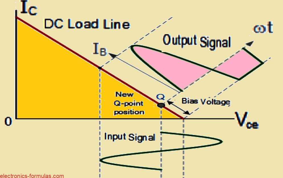
What we are doing with this pre biasing is shifting the amplifiers Q point. Think of the Q point as the amplifiers starting position. We are pushing it past the original cutoff point. The cutoff point is where the transistor is essentially “OFF.”
Extending the Active Region
By pushing the Q point past this cutoff we allow each transistor to operate in its active region for a little bit longer. Specifically it operates for slightly more than half of each cycle or more than 180 degrees. To put it simply we get 180 degrees of operation plus a little extra thanks to the bias 180° + Bias.
Class AB Amplifier
Now the amount of biasing voltage that is present at the transistors base can be increased by adding more diodes in series. Think of it like stacking batteries to get more voltage.
When we do this we create a special kind of amplifier circuit commonly known as a Class AB Amplifier.
This type of amplifier has a specific biasing arrangement which helps it operate efficiently and with less distortion.
Output Characteristics of Class AB Amplifier
Conclusions
Okay so let us break down crossover distortion and amplifier classes in a way that is easy to understand.
Essentially crossover distortion happens in Class B amplifiers because of how they are set up.
The amplifier is biased right at its cutoff point which means that when the signal we are amplifying crosses the zero axis both transistors in the amplifier briefly switch “OFF” at the same time. This creates a little gap or distortion in the output signal.
However we can fix this. By applying a small base bias voltage either with a resistive potential divider circuit or diode biasing we can minimize or even get rid of this crossover distortion.
This bias voltage brings the transistors to the point where they are just barely switched “ON” even when there is no input signal.
When we add this biasing voltage we create what is called a Class AB Amplifier. So the main difference between a Class B amplifier and a Class AB amplifier is simply the level of bias we apply to the output transistors.
One cool thing about using diodes for biasing is that their PN junctions can automatically adjust for temperature changes in the transistors. This helps keep the amplifier working consistently even if the temperature fluctuates.
So to put it simply a Class AB amplifier is really just a Class B amplifier with some added “Bias”. Here is a quick summary:
- Class A Amplifiers: No Crossover Distortion as they are biased right in the middle of their operating range.
- Class B Amplifiers: These have a lot of crossover distortion because they are biased at the cutoff point.
- Class AB Amplifiers: These might have some crossover distortion if the bias is set too low but generally it is much less than in Class B amplifiers.
Along with these three amplifier classes there are also other types of high efficiency amplifier designs.
These types of designs use different switching techniques to reduce power loss and increase efficiency. Some of them use things like RLC resonators or multiple power supply voltages to help to minimize power loss and distortion.
References:
What is crossover distortion in a push/pull amplifier?
Leave a Reply