The goal of any BJT amplifier is to keep the DC biased input voltage steady and to make the AC signal bigger.
To do this we use something called an “emitter resistance” that connects to the emitter part of a transistor. This helps the amplifier stay stable with its bias.
The stability happens because the emitter resistance gives the right amount of automatic biasing for a common emitter amplifier. To understand this better let us look at a basic amplifier circuit.
Fundamental Common Emitter BJT Amplifier Circuit
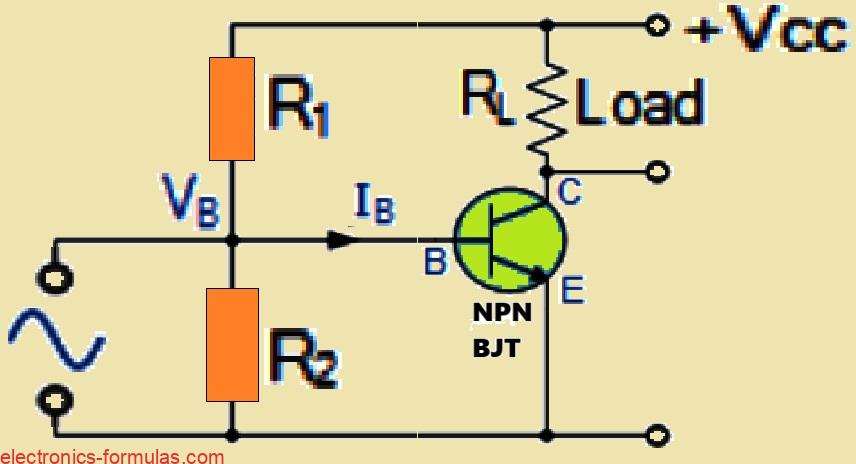
We can observe that the common emitter amplifier circuit we are looking at makes use of a voltage divider network to set the bias for the transistors base.
The common emitter configuration is a really favored approach when we are designing bipolar junction transistor amplifiers. A key aspect to remember about this circuit is that a notable amount of current makes its way into the base of the transistor.
The voltage that we find at the meeting point of our two biasing resistors which we call R1 and R2 is responsible for keeping the transistors base voltage or VB steady at a certain voltage.
This voltage is related to the supply voltage VCC. It is worth keeping in mind that VB is the voltage we measure from the base all the way to the ground which is also the same as the voltage drop we see across R2.
We generally design this class A type amplifier circuit in a way so that the base current Ib stays below 10% of the current that is flowing through the biasing resistor R2.
Let us say we need a quiescent collector current of 1mA. In that case the base current IB will be about one hundredth of that amount or 10μA. So the current that flows through resistor R2 in our potential divider network should be at least ten times that amount giving us 100μA.
The great thing about using a voltage divider is how stable it is. Because the voltage divider that R1 and R2 create is not under a heavy load, we can easily figure out the base voltage Vb by using the regular voltage divider formula.
Formula for Calculating Voltage Divider
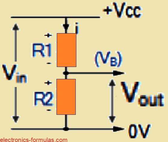
Voltage Divider Equation
Vout = Vin * (R2 / (R1 + R2))
∴ VB = VCC * (R2 / (R1 + R2))
In this particular biasing setup, we find that the base current is so small that it does not really affect the voltage divider network. Because of this if the supply voltage Vcc, happens to fluctuate or change then the voltage at the base of the transistor will also change in a directly proportional way.
Consequently we usually need some method to stabilize the transistor’s base bias or Q-point, to keep it steady.
How to Stabilize the BJT Emitter Resistance
We can make sure the amplifiers bias voltage stays steady by putting just one resistor into the transistor’s emitter circuit. You will see it in the diagrams. We call this resistor the Emitter Resistance or RE for short.
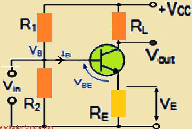
By putting in this emitter resistor we are no longer connecting the transistor’s emitter directly to ground (which is zero volts). Instead we lift it up to a little voltage above ground. We can figure out this voltage VE, using Ohm’s Law: it is simply the Emitter Current (IE) multiplied by the Emitter Resistance (RE) so VE = IE x RE.
Now let us say our Supply Voltage (Vcc) goes up. When this happens the Collector Current (Ic) of the transistor also tends to increase for a given Load Resistance.
If the collector current goes up, the emitter current also has to increase. When the emitter current increases it causes a bigger voltage drop across our emitter resistor, RE. This makes the voltage at the base (VB) rise as well, because VB = VE + VBE.
But here is the clever part, the voltage at the base is kept pretty steady by those divider resistors R1 and R2. So if VB tries to rise because of the increased VE, the voltage difference between the base and the emitter (Vbe) gets smaller.
This smaller Vbe reduces the Base Current which then stops the Collector Current from increasing even more. The same thing happens in reverse if the Supply Voltage and Collector Current try to decrease.
So what we are really doing with this emitter resistor is using negative feedback to control the base biasing of the transistor. Any changes in the collector current gets fought back by adjustments in the base bias voltage which keeps the circuit stable at a certain level.
One more thing, because some of the supply voltage gets used up by RE, we do not want RE to be too big. We want to maximize the voltage we have available across the Load Resistance (RL) to get a good output signal.
However we cannot make the value of RE super small, as this would cause instability within the circuit.
So now we can calculate the current passing through the emitter resistor using the formula as explained below:
Calculating Current through the Emitter Resistor
IE = VE/RE = (VB – VBE) / RE
∴ IE = (VB – VBE) / RE
Generally speaking when we are designing this circuit, we usually consider the voltage drop across the emitter resistance (that is RE) to be approximately equal to VB – VBE. Or, to keep things simple we can think of it as being about one-tenth (1/10th) of the supply voltage, which we call Vcc.
A typical value that we often use for the voltage across the emitter resistor is somewhere between 1 and 2 volts. We usually choose the lower of those two values.
Now we can also figure out the value of the emitter resistance RE, if we know the gain of the circuit. That is because the AC voltage gain is basically the same as the load resistance (RL) divided by the emitter resistance (RE). So by knowing the gain and RL we can easily find RE.
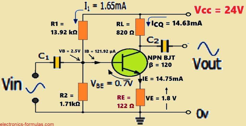
Solving a BJT Amplifier Emitter Resistance Problem #1
Assume a common emitter BJT amplifier has a current gain Beta (β) of 120. The supply voltage Vcc is 24V volts. And the load resistance RL is 820Ω.
Now to make this amplifier more stable and less sensitive to changes we have used an emitter resistance. So we want to calculate what value of resistance we should use for that emitter resistor (RE)??
We can calculate the amplifiers quiescent current ICQ in the following way:
Collector current (ICQ):
ICQ = (1/2) * Vcc / RL
= (1/2) * 24V / 820Ω
ICQ = 14.63mA
Base current (IB):
IB = ICQ / β
= 14.63mA / 120
IB = 121.92µA
Normally we can select the voltage drop across the emitter resistance to be somewhere between 1 and 2 volts, so we will assume a voltage drop VE to be 1.8 volts.
Base voltage (VB):
VB = VE + VBE
= 1.8V + 0.7V
VB = 2.5V
Resistor R2:
R2 = VB / (12 * IB)
= 2.5V / (12 * 121.92µA)
R2 = 1.71kΩ
Resistor R1:
R1 = (Vcc – VB) / (13 * IB)
= (24V – 2.5V) / (13 * 121.92µA)
R1 = 13.92kΩ
Emitter current (IE):
IE = ICQ + IB
= 14.63mA + 121.92µA
IE = 14.75mA
The emitter resistor RE can be calculated using the formula:
RE = VE / IE
Substituting the values we get:
RE = 1.8V / 14.75mA
RE = 122.03Ω
So the emitter resistor RE is approximately, 122Ω…
Using the above calculated values, we can finally draw our BJT Common Emitter Amplifier Circuit, as shown below:
In case you are interested to find the gain of the amplifier circuit, then you can do so using the following equation:
Gain (A) = RL / RE = 820 / 122 = 6.72
What is Emitter Bypass Capacitor in a BJT Amplifier Circuit

To tackle the problem of unwanted gain reduction at lower frequencies we use a special type of capacitor called the “Emitter Bypass Capacitor” CE. We connect this CE across the emitter resistance in our amplifier circuit just like in the diagram.
The clever thing about this bypass capacitor is that it makes the amplifier’s frequency response change at a specific point ƒc. It does this by effectively “bypassing” the signal currents sending them to ground instead of through the emitter resistor – that is where it gets its name.
Now because the Emitter Bypass Capacitor is a capacitor, it acts like a roadblock or an open circuit for the DC bias. This is important because it means that adding the bypass capacitor does not mess up the carefully set DC currents and voltages that keep our amplifier working correctly.
However when we look at the amplifier’s range of operating frequencies we see that the capacitors reactance XC behaves differently. At very low frequencies XC becomes extremely high. When this happens it creates a negative feedback effect which in turn causes the amplifier’s gain to drop.
To get around this issue, we carefully choose the value of our bypass capacitor CE. Generally we want its capacitive reactance to be no more than one-tenth (1/10th) of the value of the emitter resistor RE at the lowest cut-off frequency point.
So let us say that the lowest signal frequency we want to amplify is 100 Hz. Based on this we can calculate the value we need for the bypass capacitor CE, as shown below:
XC = 1/10 * RE at f3dB
= 0.1 * 122Ω
= 12.2Ω
CE = 1 / (2π * f3dB * XC)
= 1 / (2π * 100 * 12.2)
= 130 μF
That means that the emitter bypass capacitor which is linked in parallel with the emitter resistance is 130 μF for our basic common emitter amplifier circuit above.
Understanding Split Emitter Resistors
In the emitter leg of our circuit we have divided the resistor into two separate parts which RE1 and RE2. This creates a voltage divider network within the emitter leg. Additionally we have connected a bypass capacitor across the lower resistor RE2 in parallel.
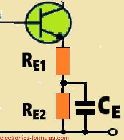
Now looking at the two resistors individually RE1 the upper resistor remains unchanged in value compared to the original circuit. However since it is not bypassed by the capacitor it must still be taken into account when we calculate the signal parameters.
On the other hand the lower resistor RE2 is directly in parallel with the capacitor. At high frequencies this capacitor effectively acts as a short circuit, meaning RE2 is essentially reduced to zero ohms for AC signal calculations.
The key advantage of this configuration is that we now have control over the AC gain of the amplifier across the entire frequency range.
At DC the total emitter resistance is simply the sum of both resistors RE1 + RE2. However at higher AC frequencies the effect of the capacitor shorting out RE2 means that only RE1 contributes to the emitter resistance.
In other words at high frequencies the circuit behaves just like our original design where the emitter resistor was fully unbypassed.
This raises an important question, How do we determine the value of RE2? The answer depends on the desired DC voltage gain at the lower frequency cut-off point. We previously established that the gain of the original common emitter circuit was given by the ratio:
Gain = RL / RE
For our earlier design this was calculated as 10 using 1kΩ for RL and 100Ω for RE. However with the new emitter resistance configuration the gain at DC is now determined by:
Gain = RL / (RE1 + RE2)
By carefully selecting RE2, we can fine-tune the gain response at different frequencies, allowing for more precise control over the amplifiers performance.
As a result, the emitter resistor RE2 obtains the following amount once you select a DC gain of , for example a 1 (one):
DC Gain, (Adc) = RL / (RE1 + RE2),
so, 820 Ω / (122 Ω + RE2) = 1
Therefore, RE2 = (RL / Adc – RE1)
= (820 Ω / 1) – 122 Ω
= 698 Ω
So if we aim for a DC gain of exactly maybe 1 (one), then we set RE1 to 122Ω and RE2 to 698Ω. It is important to note that the AC gain still remains unchanged at 6.72.
In this case a split-emitter amplifier will have its voltage gain and input impedance positioned between the values seen in a fully bypassed emitter amplifier and an unbypassed emitter amplifier. The exact characteristics will depends on the operating frequency.
Conclusions
So when we use a transistor, its current amplification parameter called β isn’t always the same. Even if we pick two transistors with the same type and part number they might still have different β values. This happens because of tiny differences in how they are made. Also, β can change if the supply voltage or the temperature goes up or down.
Now in a common emitter class-A amplifier circuit we need a biasing circuit to keep the Q-point steady. This helps make sure the DC collector current IC doesn’t depend on β too much. One way to do this is by adding something called an Emitter Resistance RE in the emitter leg which helps stabilize everything.
Usually the voltage drop across this emitter resistance is between 1 to 2 volts. If we want a higher AC gain, we can completely bypass this resistor using a bypass capacitor CE. This capacitor is placed in parallel with RE.
But if we only partly bypass it using a split-emitter voltage divider network we can reduce DC gain and distortion. The size of this capacitor depends on its capacitive reactance (XC) at the lowest signal frequency.
References:
What is the purpose of the emitter resistor in a common emitter amplifier?
Emitter Resistors – in amplifer power circuit
Leave a Reply